


")

The proposed device is designed to protect equipment that consume DC voltage significant pulse current (USC, transceivers, etc.). The device disconnects the load in cases of excessive raising or lowering of the supply voltage. The thresholds of protection can be adjusted within wide limits. Small dimensions of the device allow you to plug it into a powered load.
When a powerful low-voltage apparatus receives power from non-random sources, including automotive batteries, its very urgent protection against polarity reversal and invalid supply voltage (too high or too low). In the first case it is possible to apply the classical method - fuse and powerful diode cathode connected to the positive and the anode to the negative power bus. For the second case, developed the device, which plugs into the power system load and can be embedded in the load. Diagram of the device shown in Fig. 1.
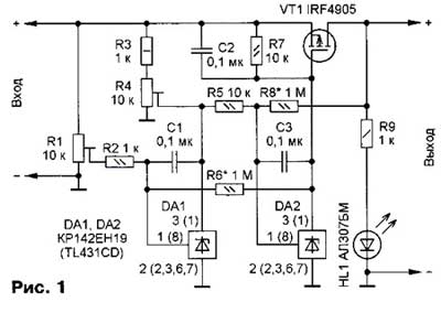
Load commutes powerful key of a p-channel field-effect transistor IRF4905 ( VT1) run two circuits - parallel voltage regulators - CRIN ( DA1 and DA2), operating in the mode of the comparator. If the voltage on the input circuit KREN less threshold shift (2.5 V), the chip is closed and consumes a current of about 1 μa. Otherwise, the current through the chip increases dramatically (with a slope of approximately 2 A/b), therefore, his limit external elements so that it does not exceed 100 mA. The assembled chip DA1 node responsive to the supply voltage increases, and DA2 - down. Characteristics of the device shown in Fig. 2.
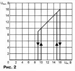
Consider a smooth increase of the supply voltage. While it is less than 10, both circuits are closed and the current through the resistor R7 is small. The voltage on this resistor is not sufficient to open the transistor VT1, the load is disconnected, the led is not lit HL1. When the supply voltage will increase to 10 V, the voltage on the control input circuit DA2 reaches 2.5 V and the chip will open. The current through it increases, the voltage across the resistor R7 will increase, and the transistor will open and connect the load. The low open channel resistance of the transistor VT1 (0.02 Ω) the voltage drop will be low and almost all the input voltage is supplied to the load. HL1 led indicates the enabled state of the load. When the voltage reaches 16 V, opens chip DA 1, the voltage across it does not exceed 2 V, resulting in chip DA 2 is closed, the transistor VT1 is also closed and turn off the load. HL1 led will go out.
With a smooth decrease in supply voltage, the load will be turned on when a voltage of 15 V and disabled when 9 V. Thus, each switching threshold has a hysteresis, which increases the reliability of the switch and eliminates the repeated switching of the load when the power supply voltage instability hesitates at the threshold. The upper hysteresis threshold implemented with positive feedback through the resistor R6, the lower threshold through resistor R8. The above thresholds may be modified within wide limits: upper - trimming resistor R1, the lower - R4. The increase in the resistance of resistors R 6 reduces the hysteresis upper threshold, R 8 is lower. To reduce the influence of noise in the negative feedback circuit chip includes the capacitors C1 and C3, but be aware that they reduce the speed of the device. At load current 10 A voltage drop at the open transistor VT1 will not exceed 0.2 V, and power dissipation will be less than 2 watts, so the transistor can be used without a heat sink. At a current of 20 A power dissipation can be as high as 8 watts, so you need a small heat sink or turns on the two transistors in parallel. Voltage including ripple should be less than the maximum allowable voltage circuits - V. 30
Design and details
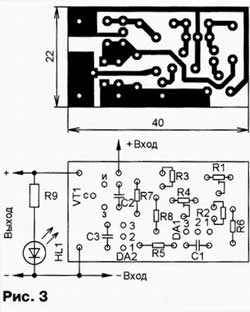
Transistor IRF 4905 ( VT 1) field with the p-channel case TO-220 or IRF4905L in the case of to-262, you can also use IRFU5305 in the body-A. Chip CRAN ( DA1 and DA2) can be replaced by foreign analogue TL CLR 431. All capacitors - K10-17 or similar import, fixed resistors - R1-4, MLT, S2-33, trimmer - SDR-19. For these details the calculated fee, the drawing of which is shown in Fig. 3. It is manufactured of one-sided foil fiberglass.
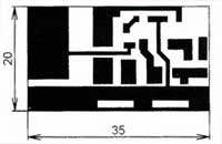
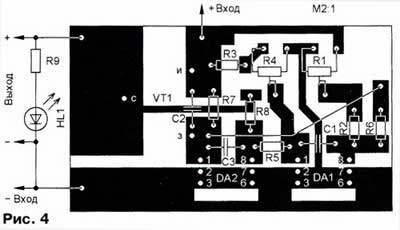
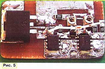
If you want to reduce the dimensions of the device, it is necessary to apply details for surface mount: transistor VT 1 IRF 4905 S - in the case D 2 - Pak or IRFR 5305 - in the case of D - Pak , circuits DA1 and DA2 TL431CD - in the case of SOP -8, trimming resistors PVZ , fixed resistors and capacitors are size 1206. Drawing of the PCB for such parts shown in Fig. 4, a photograph of the mounted Board in Fig. 5.
Led HL1, you can use any low-power visible spectrum radiation. The resistance of the resistor R 9 is selected so that at maximum voltage of load current through the led does not exceed the maximum permissible values. HL1 led and resistor R9 is set out Board mounted Assembly. These elements are needed only if the load has no indication to the enabled state.
The establishment is to install switching thresholds trimmer resistors R1 and R4, the desired values of hystereses set selection of resistors R6 and R8.
Author: I. Nechaev, Kursk; Publication: www.cxem.net