


")

To manage various kinds of electrical installations in the home and at work there is often a need for multiple on and off via some intervals. This problem usually can be solved with the help of digital timer with memory. In the article published below for the attention of readers the description of the variant of the device of such appointment, which can to make independently.
A programmable machine designed to control the network appliances low and medium (up to 1 kW) of power. In everyday life it can be used, for example, to manage Chizhevsky chandelier or electric heating appliances in residential the room. The author used the machine to control the computer, communicating with BBS in night time.
The machine contains two identical independent programmable channels, each of which controls one load. The number of channels can be arbitrary increased without fundamental modifications of the basic components of the device itself. During his work is counted real-time and display the current value in hours and minutes, as well as ordinal numbers (1 to 7) days of the week.
The maximum duration of the control program in each of the channels is one day, however, if necessary, the user can allow or deny the fulfillment is recorded in the memory of the daily program in any of the seven days of the week. Minimum programmable interval between two events is one minute. Under the event is on or off controlled load. Thus, the maximum number of programmable events is equal to the number of minutes in a day, i.e. 1440. At any time through the organs control you can change the current state of the loads. The clearing of memory before programming automatically selects addresses on command user in both channels at once or each separately.
When programming provides for the possibility pogresno recording and Podrezkovo erasing data in memory. The dispenser has a generator AF, which can beep in the moments of occurrence of each programmed events. When disconnecting the mains voltage is provided auto switch digital (low voltage) side of the device powered by a backup battery that allows you to keep continuous track of time, and to avoid the change of the current States governing loads of triggers.
Block diagram of the machine shown in Fig. 1. It consists of a unit of account and indication, two identical channel blocks, electronic relay, and generator CC, which can be connected to any of the channels (in the diagram, for example, for channel 1).
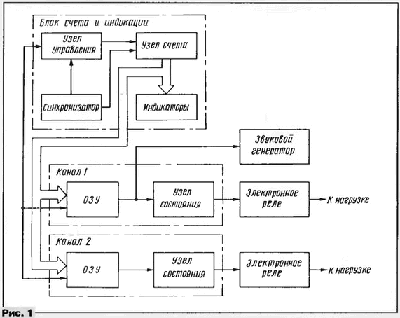
In the unit of account and the display is counting the current time and day of the week display their values on the indicators, as well as the formation of addresses for RAM channels.
The management node sets the counters in the right position and makes operations with memory channels. The synchronizer generates the counting and control the sequence of pulses. RAM stores the program state management loads in each channel. Nodes status transform read from RAM the pulse voltage signals in a certain logical level, which control electronic relays, switching input to the load network voltage.
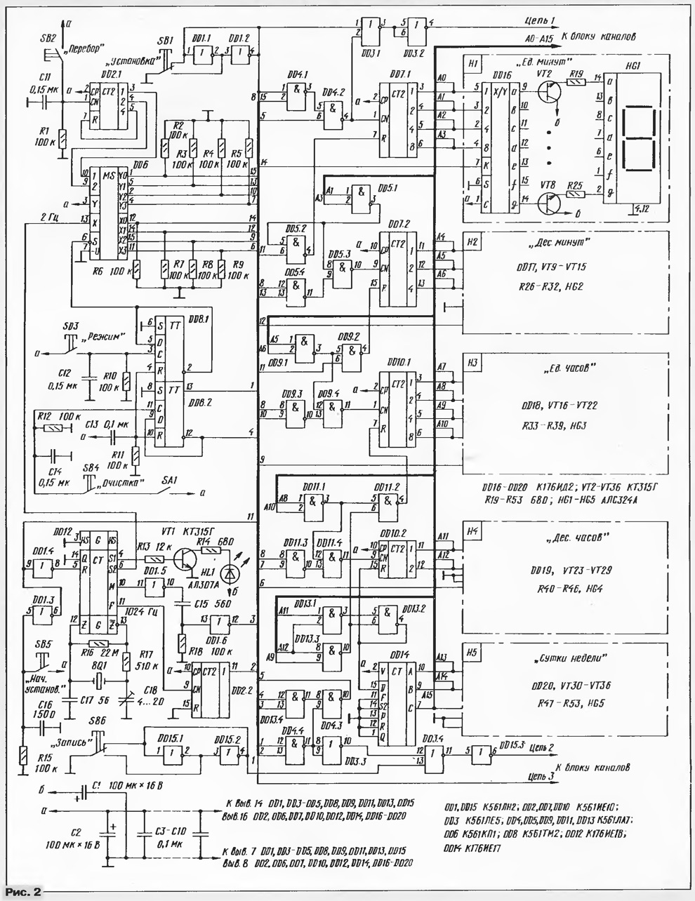
Schematic diagram of the unit of account and display unit shown in Fig. 2. It is an electronic watch. Features counting and control sequences of pulses (synchronizer) performs in them specialized clock chip DD12 (CIE) containing quartz generator. With her findings removed the following signals: pin. 10 - counting minute pulses (1/60 Hz), which through a chain shortening on the elements DD1.5, DD1.6, C15, R18 and elements DD13.4, DD4.3, DD4.2 are received at the counting input counter units minutes DD7.1; with the pin. 4 - second pulses, used for indication of used rhythm led HL1; with the pin. 11 - pulses with a frequency of 1024 Hz, which pass through the counter-divider by two DD2.2, and the frequency of their drops to 512 Hz; with pin. 6 - pulses with a frequency of 2 Hz, providing flashing familiarity indicators HG1 - HG4 in the set up mode of their testimony.
(click to enlarge)
Counting the part of the unit constructed according to a common scheme with serial connection counters with the given conversion factors, and static indication of device status seven-segment indicators HG1 - HG5. Address bus AO - A15 formed from involved when the score digits chips DD7, DD10, DD14. Feature of the proposed circuit solutions is the ability to prompt the user changes the status of each of counters, which facilitates the entry in the data memory when programming.
Control unit buttons SB1 - "Installation", SB2 - "Bust familiarity" and SB3 is "Mode". In the initial state on the pin. 6 decoder DD6 present high logic level, therefore, all the outputs (pin. 1, 5, 2, 4, 12, 14, 15, 11) will be low, prohibiting the passage of the locating pulses from button SB1 counters DD7.1, DD7.2, DD10.1, DD10.2 through the elements of DD4.1, DD5.4, DD9.3, DD11.3 and permitting the conversion of the decoders DD16 - DD19. When once you press the button SB3 trigger DD8.1 passes in one state, allowing the operation of the switches of the decoder DD6, one of the outputs (pin. 1, 5, 2, 4) which there is a high level, and the other (pin. 12, 14, 15, 11) - pulses with a frequency of 2 Hz. As a result, one of the four familiarity HG1 - N4 flashes the specified frequency. Use the button to change the state SB1 counter of familiarity (the display). "Activity" of a familiarity depends on the state of the counter DD2.1 at the moment of pressing the button SB3. Change the state of the counter DD2.1 can button SB2. Thus, consistently setting up the indicators on each familiarity can very fast set up time required (the address on the address bus).
The counter state of day of the week DD14 is established by a transfer when you install counter status of tens of hours DD10.2. It should be noted that the installation the required reading is convenient to start with a few minutes and finish the day of the week, as the set value in the higher familiarity will incremented transfer, which can occur when setting the value in Junior familiarity. Button SB5 "setup" is intended for precise {to seconds) set the clock to a reference time source. In the moment you this button resets the internal counter of seconds chip DD12 and counters units and tens of minutes chips DD7.1, DD7.2.
In addition to the address signals AO - A15, block the account and display yet several control signals: pin. 4 chip DD3.2 (circuit 1) - short minute pulses, adjusting the pulses of the button SB1; with the pin. 6 chips DD15.3 (circuit 2) is a pulse from the button SB6 "Record", and a pulse frequency of 512 Hz (memory cleanup); + 13 chip DD8 (chain 3) static a signal that provides an implementation of the cleaning mode memory.
The clear memory mode is set by pressing the button SB4 "Cleaning" in that case, if the switch contacts unlock clean SA1 closed. In this mode, the trigger DD8.2 goes to a logic 1, the passage of minute pulses at the counting input of the counter DD7.1 through the element DD13.4 prohibited, and the passage of pulses of a frequency of 512 Hz using the element DD4.4 permitted. The result is an account {bust addresses) with a frequency of 512 Hz. Pressing the button SB4 returns trigger DD8.2 to its original state logic zero. During initial power-up both triggers DD8 are set to a logic zero chain С13R11.
Buttons SB1, SB6 have a device to prevent contact bounce, which is made on the elements DD1.1, DD1.2, DD15.1, DD15.2. Chain DD1.5, C15, R18, DD1.6 shortens a long minute pulse with a pin. 10 chip DD12. Otherwise, this the impetus for several tens of seconds in every minute would prohibit the installation counter status DD7.1 button SB1.
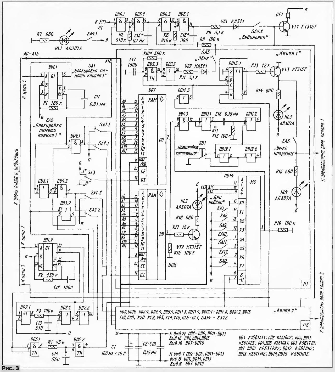
In Fig. 3 shows a schematic block diagram of a programmable channels machine. Here shows a circuit common to both channels of the device, performed on the elements DD1, DD2, DD3.1, DD3.2, DD4.1, DD4.2, DD5.1, DD5.2, which produces signals that control the memory.
Now consider the work of the first channel in the recording mode with real account time. As shown in Fig. 3, from address bus AO - A15 is assigned the category A12. From its state depends on the choice of chip RAM, which is being addressed. Suppose that at the moment this bit is in a single state and for treatment active low signal to the CE pin. 10 DD7, DD8) selected chip DD7. Chip DD8 in this case is set for release in the third state.
(click to enlarge)
When changing the address on the bus addresses AO - A15 (front minute or installation pulse coming from the unit account and display) a single-shot DD1.1 forms the high level pulse during which the address to the chip DD7 it is prohibited to avoid reading at this point data from memory. In the gaps between the pulses generated DD1 chip.1, the output of the chip DD7 (vyv. 7) set the logical level corresponding to the bit data read at your current address.
To record a data bit in the memory according to the address, a user must set his bus control buttons of the unit of account and indication. Then switch SA3 you should select the suggested entry level: a logical zero or a logical unit. In the case of unit selection in memory will be written to the event, which will happen at a set time. When recording scratch is possible, for example, to erase previously recorded at this address the event. Next you need to click once the button SB6 "Record" (see Fig. 2). On the front of the momentum along the chain 2 will arrive on a single-shot DD1.2, the latter generates at its outputs the pulses record (Fig. 4,a).
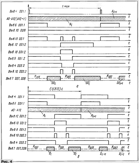
With direct access DD1 chip.2 (vyv. 10) impulse records arrives at the site of generation of short pulses at the front and the decay of the pulse recordings made on the elements DD2.1, R3, C13, DD2.2, DD2.3. With inverse the output circuits DD1.2 (vyv. 9) writing pulse hits the node delay on the elements DD5.1, R4, C14, DD5.2, and then on the pin. 8 memory chips DD7, DD8. The delay time is chosen so that the moments of the differential signal (pulse) record on the pin. 8 chip DD7 appeal to it was forbidden entering her pin. 10 short pulses with pin. 10 chip DD2.3. Thus creates the necessary conditions for the correct operation of clocked RAM chips CRRU in compliance with the passport regime [1]. After the second short pulse with the pin. 10 chip DD2.3 on the pin. 7 chip DD7 set the logical level corresponding to the just recorded bat data (Fig. 4,a).
The bits A13 - A15 counter day of the week (see Fig. 2) on the memory chips not act, and served on the decoder DD14 as address, dial-up the electronic key chip. The inputs of electronic switches DD14(vyv. 14, 15, 12, 1, 5, 2, 4) and switches SA7-SA13 correspond to the days of the week, Monday to Sunday. If one of the switches in the corresponding day of the week closed, high voltage is present at the pin. 3 chip DD14, allow the passage of a high logic level to the pin. 7 RAM DD7, DD8 via chip DD4.3. When the open state of the switches low the level on the pin. 3 chip DD14 prohibits the above passage. Chain C18R12 forms the edge read from the memory voltage high-level impulse trigger the loading condition DD13.1. The user can any time change the state of the trigger button SB1, controlling it the presence or absence of luminescence of the led HL3. If programming is produced when the load is connected, it should be temporarily disabled switch SA6. The control condition produced by the LEDs HL4. Whenever the input (pin. 3) trigger DD13.1 impulse comes switching the phone BF1 hear a short beep (high tone) generated by the generator 3H on the elements R17, R10, DD5.3, DD3.3.
Before writing programs in memory should be clear, i.e. to record all available addresses are logical zeros. Bust addresses when cleaning is performed with the relatively low frequency of 512 Hz (Fig. 4,b), which allows visually (on the lack of blinking LEDs HL2) and aurally (by the disappearance of the signal playing telephone BF1) control in the absence of logical memory units. Cleaning cycle (over all possible time values) should be repeated 2-3 times. It only takes a few seconds. The switch should be SA3 pre-set to "0". If you want to work with memory only one channel without affecting the contents of the memory of the other, it is possible to block the latter from the treatment of the translation of the corresponding switch SA1 or SA2 "memory Lock" in the bottom according to the scheme position. During the cleaning mode triggers the loading condition DD13.1 and DD13.2 in both channels are converted into the logic zero state by a high level on the R-input (pin. 4 and 10). Sound generator alarm made on the chip DD6, the enable input (pin. 1 DD6) connects to the pin. 3 chip DD11.1 of the first or the pin. 10 chips DD11.3 second channel. In case of reading from the memory a high level in a predetermined the time when the closed switch SA4 Alarm intermittent alarm will sound in for one minute.
Schematic diagram of the electronic relay and power supply programmable machine shown in Fig. 5. The digital part of the electronic relay is made on the basis the devices described in [3]. As the power electronic relay elements used triac switches VS1, VS2, which is a disadvantage the presence of switching emissions and distortion sinusoidal current when management powerful reactive loads. In the proposed device load commutes in the moment of transition of the AC mains voltage through zero, therefore, when switching a purely resistive loads emissions from managed to get rid of.
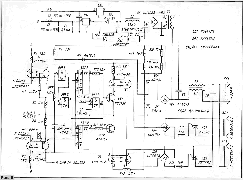
(click to enlarge)
Timing diagrams illustrating the operation of the electronic relay, presented at Fig. 6.
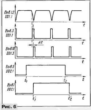
Positive differential voltage is supplied to turn on the load the input D of the trigger pin. 5 DD2.1) at an arbitrary time t1, will be transferred to the output (vyv. 1 DD2.1) only in the time of arrival to its input (pin. 3 DD2.1) short pulse that coincides with the transition of the mains voltage through zero. The presence of node delay short pulse on the elements DD1.2, R9, C7, DD1.3 not is mandatory and basic, but allows it to be aligned on time the leading edge of a pulse received at the input With trigger point the transition of the mains voltage through zero (failure pulsating voltage findings 1, 2 DD1 chip.1).
The use of opto-couplers U1 - U4 allowed to fully unleash unit e the relay and the digital part of the machine.
The power supply has two integral stabilizer DA1 and DA2. The first of them supplies the digital part of the machine. Its input voltage redundant battery GB1 chain automatic switching diodes VD2, VD3. The second regulator is used to power the optocouplers, LEDs and seven-segment indicators. The network filter C8L2L3C9 suppresses emissions and noise the mains voltage.
To the base of the machine rigid requirements.
The author used the resistors OMLT specified on the power schemes, oxide the capacitors C50-16, rest km, KLS; button SB1 - SB6 (see Fig. 2) and SB1, SB2 (see Fig.3) - BM1-1; switches SA1, SA2 (see Fig. 3) - MTW, SA3, SA6, SA15 (see Fig. 3) and SA1 (see Fig. 2) - MT, SA4 (see Fig. 3), SA1(cm. Fig. 5) - PC4-1, switches "Days of week" SA7 - SA13, SA16 - SA22 - Assembly microswitches VDM-8. The eighth switch Assembly is used as SA5, SA14 ("Sound"). Seven-segment led indicators with any common cathode (better to use imported, for example, LTS547AP). Transistors KT315 with any letter index, a quartz resonator BQ 1 at a frequency of 32 768 Hz, telephone the primer BF1 - any resistance 200…300 Ohm, for example, import DH30F. Triacs COG can be replaced by more powerful, for example, TS-16-10-7, but distortion sinusoidal current control of inductive loads in this case more noticeable. As an electronic relay can be used integral solid-state relay" D2410 or D2475 IR firm in which the inclusion implemented according to the mains voltage zero and off - zero current through the load [4].
The transformer T1 should ensure the secondary winding of the AC voltage about 8 V At a load current of 600 mA. Coil filters L1 - L3 are wound on the rings (20x10x4 mm) ferrite MNM-1 wire MGTF 0.5 to fill, and coils L2, L3 are wound with two wires simultaneously.
As GB1 used a battery of six finger elements. Current, consumption of the digital part of the device from the battery, in the absence of stress the network does not exceed 35 mA.
The machine is placed in body size 265x200x100 mm. On the front panel there are all the controls and display, and rear - sockets load. The triac VS1, VS2 installed on a heat sink with an area of about 150 cm2, and stabilizer DA2 - on heat sink area of 50 cm2.
The unit of account and the display and the unit channels are mounted on separate circuit boards dimensions 185x80 mm, elements of electronic relays (except triac VS1, VS2) and power supply (except for the capacitors C1 - C3, circuits DA1, DA2, GB1 battery and transformer T1) placed on a common motherboard sizes 170x80 mm. Capacitors C3-C10 in the block account and indication and C2-C10 in the block of channels is soldered between pins "General" and "plus power" RAM chips, counters, and triggers.
With proper parts and proper installation, the digital part of the machine starts to work immediately. The establishment of the unit of account and indication comes down to tuning the frequency of the crystal oscillator on the chip DD12 capacitor C18. When the building block of channels, the selection of resistors R10, R20 should be set the tone channel sound generators, and the selection of the capacitor C16 is generator alarm. Desired duration of the alarm alerts choose a capacitor C15. When establishing the unit of electronic relays should select resistor R8 so that the pulse low level input Schmitt trigger DD1.1 (vyv. 1, 2) provide sustainable switching. The selection of resistor R9 in the circuit delay should combine the time-front pulse on the pin. 10 DD1 chip.3 with the lower point of the pulse at the pin. 1, 2 chip DD1.1 (Fig. 6).
Getting started programming the machine, consider the following. If the program contains a large enough number of events, it is recommended to build a timing diagram in which a high level to indicate the enabled state load, low or off, and the differences between the levels of events. Panel the desired moments of the event, you should write to these addresses in the memory unit, to put indicators on the current exact time, be connected to the load device and install-click "set status" initial state of the load in accordance with the constructed graph.
When recording and monitoring data, it is impossible to use the button "Start. setup", because when you click on it the status of the address bus changes, but correct reading from the memory at the new address is not achieved.
Analyzing the operation of the machine, it is easy to see that, with the deletion of the address numbers served on-chip RAM, the bits of the counter units of minutes AO - A3 and including there a bits of the counter of the day, A13 - A15, you can get the device programmable for a week. Since the bit width of the address bus RAM will be one less, it will be possible to have one memory chip on channel, and also to eliminate decoders DD14, DD15. The minimum interval between the events in this case will be equal to ten minutes, and the maximum number events in the week program will be reduced to 144x7=1008.
Literature
Author: P. Redkin, Ulyanovsk