


")

Chip CRM is another solution to the problem of power control high voltage powerful loads. The chip can be used to smooth on and off of electric light bulbs and change the brightness glow, to control more powerful semiconductor switching devices for regulating the rotational speed of electric motors. Devices manufactured by epitaxial technology with isolation dielectric.
Of the features of the regulator should be noted is its ability to limit power in the load when reaching the maximum allowable case temperature device.
The regulator CRP decorated in plastic case-European design POWEP-DIP (12+4). It shestnadcatiletniy case (Fig. 1) with metric pitch conclusions, which conclusions 4, 5 and 12, 13 are left free. Mechanical and electrically these findings are consolidated and are designed for heat sinking from crystal. In addition to these, not used pins 1, 2, 7, 8. Unit weight - not more than 1.5 G.
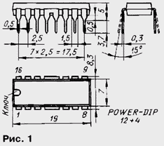
In the early stages of development of the chip in production it was released in die version and in the widespread European case DIP16.
In Fig. 2 shows a schematic diagram of the controller and the model scheme inclusion. The chip consists of two triacs, collected every scheme transistor analog SCR (VT1, VT2 and VT3, VT4) and included anti-parallel, and a management node (VT5-VT17). The output of the management node is associated with management's conclusions triacs dividing diodes VD6, VD7.
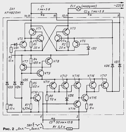
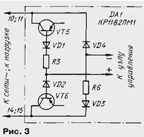
The management node is powered by a diode bridge-connected AC voltage network findings 14, 15, and 10, 11 of the chip. The bridge configuration somewhat different from the traditional (Fig. 3). Resistors R3 and R6 play a role ballast.
External capacitors C1, C2 provide the necessary turn-on delay the triacs at each wave of the mains voltage relative to the time of his crossing the "zero". These capacitors also do not allow the triacs to open at the time of filing of the mains voltage.
The management node, in turn, consists of a stabilized power supply transistors VT7-VT9, current generator transistors VT11, VT12, charges the external timing capacitor C3, the voltage-to-current transistor VT13-VT15 and "current mirror" VT16-VT17. Transistor VT10 and the resistors R5, R7 assembled device thermal protection chip.
In Fig. 2 as an example, shows a diagram of the external control circuit elements C3, R1, SB1 - to use the controller in the device soft start and turn off the lights EL1. The power controller operates as way. When applying mains voltage triacs VT1, VT2 and VT3, VT4 closed. On the management node from the power source receives a supply voltage of 6.3 V and it produces some output current IOUT (the collector current of the transistor VT17).
Suppose that at the current moment at the joint findings 14, 15 positive voltage, and 10, 11 are negative. Output current management node chips through the diode VD7 will charge late in the capacitor C2. Through some time the voltage on this capacitor will increase to a level at which open SCR VT1, VT2.
From now until the end of halftime through the load - lamp EL1 - will leaking current, a rectifier bridge feeding the host government will be shunted open SCR. Capacitor C1 remains discharged.
After changing the polarity of the mains voltage and starts charging the capacitor C1 and with the same delay open SCR VT3, VT4. The capacitor C2 during the this halftime is rapidly discharged through the resistor R1 and the transistor VT5.
In Fig. 4 shows timing diagrams of the voltages on the capacitors C1 and C2. The solid lines show the processes described above, some relevant the intermediate value of the output current management node. It is seen that the opening the triacs occurs when the voltage on the capacitors C1, C2, equal to 0.7 V. The shape of the load voltage shown in Fig. 4,
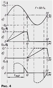
Delayed switch-on of the triacs in seconds relative to the beginning of the half cycle is equal to tзад=0,S/IOUT, where 0.7 V is the threshold voltage of opening triacs; C2=C1 - capacity check capacitor (microfarad); IOUT - output current (in µa) of the management node.
If you change the output current of the management node will change turn-on delay the triacs in each half-cycle of mains voltage, and hence power, eye-catching in the load. In Fig. 4 this is illustrated by the bold dashed lines. If the minimum value of the output current IOUT min delay should to exceed half of the period.
In the first few half-cycles after the filing of the regulator (Fig. 2) network the discharged voltage of the timing capacitor C3 closes conclusions 3 and 6 chips like a wire jumper, so the output current IOUT=IOUT min. However, since the current generator transistors VT11, VT12, the resistor R8 and the diode VD8 provides stable current flowing through the pin 6, capacitor C3 smoothly charged.
This leads to an increase of the voltage on the base of the transistor VT14, which transistor VT15 starts to open. As a result the output current of the management node increases, the delay time of the triacs in each successive half cycle decreases the brightness of the lamp EL1 smoothly increases from zero to maximum.
If you now close the contacts of switch SB1, the capacitor C3 will be discharged through the resistor R1 and the brightness of the lamp to decrease until complete extinction. Discharge current capacitor should be greater than the current charge from the pin 6 of the chip.
Main technical characteristics at Tamb.SR=25°C
Current consumption, mA, not more, with dial-up voltage 400 V and the voltage of the control input (pin. 6)
zero
6 In
2
5 The saturation voltage of the open SCR, no more, at a current load 0.5 A 2 The input current is flowing the control input, µa, at zero the voltage across it and dial-up voltage 100 V 40…150 The output current of the SCR control unit, mA, with dial-up a voltage of 100 V and the voltage of the control input
zero, no more
3 In
6 In
0,2
0,15 0,9…
0,4…1,2 The leakage current control input, the ICA, not more, when the voltage on it 6 In and zero dial-up voltage 30 The frequency of the mains voltage, Hz 40…70 Thermal resistance, °C/W, not more
crystal-heat-conclusions
crystal-environment
14
80 Operating range ambient temperature, °C -40…+70 Storage temperature, °C -55…+150
Maximum operating values
Voltage (RMS), 80…276 The highest load current, And 1,2 The greatest load capacity, W 150 The dissipated power, W, not more, at a temperatureheat conclusions 90°C
ambient 70°C
4
1 The highest voltage of static electricity, 500
The lack of active closing of triacs allows the chip to use her to control the power inductive load, because after the transition the phase of the mains voltage through zero, the corresponding SCR will remain open until the complete cessation of current through the load.
To ensure the normal operation of the power control, it is necessary to determine the minimum and maximum output current of the node management chip. So, to delay the opening of the triacs 10 MS with capacity C1=C2=1 µf and threshold start voltage of 0.7 In the above formula gives the value minimum output current of about 70 mA.
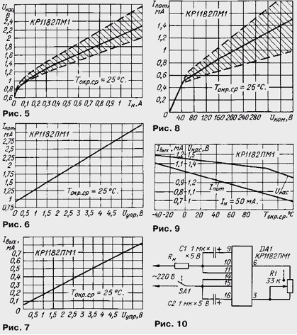
In Fig. 5-9 presents the main graphical based operating characteristics chipset series CRM. The dependence of the saturation voltage the triacs chips on the load current shown in Fig. 5; on this and other figures the hatched area of technological spread. In Fig. 6 and 7 shows the dependence of the consumed current and the control current of the triacs from the tension the control input of the chip (pin. 6).
Fig. 8 shows the dependence of the consumed chip current values from dial-up voltage, and in Fig. 9 shows temperature characteristics saturation voltage of the triacs and current management.
The main circuit of the controller CRP presented in Fig. 2. When open contacts of the switch SB1 supply mains voltage lamp EL1 turns on smoothly after opening - goes off smoothly.
By changing the capacitance of the timing capacitor C3 from 20 to 100 UF, you can change turn-on time from a few tenths of a second (visually imperceptible smoothness, but the thread the lamp will be protected from excessive inrush current) 1 a…2 s. the Time off set by selection of resistor R1 in the range from 47 Ohms to several of the shortfall.
In Fig. 10 shows a diagram of the manual power control of an incandescent lamp, the soldering iron or the frequency of rotation of a household fan. Here network the switch SA1 is desirable to combine with level control power resistor R1, and the contacts SA1 should be opened after the installation of the engine resistor R1 in the position of minimum resistance, which corresponds to the off load. In this position should enable the controller to the network.
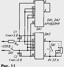
Chip CRM allow parallel connection of two or more devices. It allows you to increase the power output of the regulator. So, device, scheme which is shown in Fig. 11, can work with the load RL with a capacity of up to 300 W. The number of hinged elements in parallel circuits remains still.
It is easy to see that both triacs regulators DA1 and DA2 open the voltage generated by the chip of DA2. Control outputs 6 and 3 all additional regulators close.
With a significant power load may be that the construction of the switch SA1, combined with an adjusting resistor R1 does not designed for such a large current. In this case it is necessary to slightly modify the scheme, moving the switch controller in the control circuit, as shown in Fig. 11 dashed lines.
Note that in the new circuit embodiment, the controller is switched off when the contacts SA1 closed (not open as in the original). To enable this controller to the network it is necessary when the closed contacts SA1 and at the position of minimum resistance adjustment of the resistor R1. Before switching off the load, it is desirable to reduce to low power on it, setting the slider to the resistor R1 in upper circuit position.
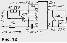
Strong increase load power (up to 1 kW) can be achieved by introducing into the regulator is a powerful discrete triac VS1 (Fig. 12).
When using the controller CRM for brightness control of incandescent lamps it must be remembered that the cold resistance of the spiral lamp is almost 10 times less than scorching. Because of this, the amplitude of the current at the moment the mains lamp power 150 W can reach 10 A. Design the chip allows the current from within just units of microseconds, whereas the heating of the spiral continued for several half-cycles of the mains voltage.
At the recommended values of the external control circuit of the filament for a smooth on and off the bulb (see Fig. 2) the current through the lamp power 150 watts for the whole process of its inclusion does not exceed 2…2,5 A.
Author: A. Nemec, Bryansk