


")

Description
Described here, the infrared control system has high noise immunity, which is achieved by multiple transfer commands. In this case, the decoder sends a signal of reception of the corresponding command only in the case when at least two of three consecutive received command contains the same information.
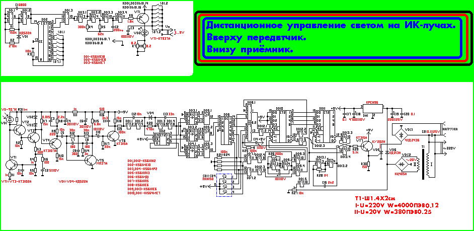
Transmitter
For sending commands used impulse-number code. Encoder transmitter is built on two digital mos IC series 561 (Fig.1, DD1, DD2). On the elements DD1.1 and DD1.2 is assembled, the generator of rectangular pulses, operating at a frequency of about 200 Hz. Due to the fact that the switching threshold of the CMOS elements does not correspond to exactly half the supply voltage balancing pulses in a traditional scheme generator added elements R2 and VD1 .
The pulse generator are fed to the counter with the decoder (chip DD2), normally having a conversion factor of 10. In those moments, when the counter is in state 0 or 1, the pins 0 or 1 (pins 3 or 2 respectively) logical 1 is present, which prevents the passage of pulses of the generator through the element DD1.3 on the buffer element of the transmitter. For other States of the counter pulses of positive polarity are held in a buffer element of the transmitter. As a result, if you do not press any of the buttons SB1-SB7, the buffer element of the transmitter come in packs of eight pulses separated by an interval equal to 2.5 period pulses. The transfer of the packets corresponds to the lack of teams.
(click to enlarge)
Let us consider the formation of teams for example team, containing 5 pulses. If you press the button SB5 , the counter, as before, prevents the passage of the modulator of the first two pulses. Then to the transmit buffer are 5 pulses, after which the counter is set to 7 and at its output 7 (pin 6 DD2) is set logic 1. This signal through the closed contacts of the button SB5 is fed to the input R of the counter DD2 and resets it to 0. As a result, the output 10 of the element DD1.3 are formed of bundles of five pulses separated by intervals of the same duration and in the absence of a transfer command.
When I press any other button packs are generated corresponding to the number buttons the number of pulses from one to eight, separated by the same interval.
The IR transmitter is a buffer element (DD3.1, DD3.2), the carrier frequency generator (25-30 kHz.)(DD3.3,DD3.4) and an amplifier (VT1). The carrier frequency generator is simulated by amplitude bursts of pulses from the encoder. In the collector circuit of the transistor VT1 is connected to the infrared emitting led, and he sends in the space of an exact copy of the encoder signal.
Receiver
The receiver is built on the classical scheme adopted in the Russian industry (particularly in TVs Rubin, Tempo, etc.). The pulses of infrared radiation appear on an infrared photodiode VD1 , is converted into electrical signals and amplified by transistors VT3, VT4, which is connected in the circuit with common emitter. On the VT2 transistor is assembled emitter follower, matching the dynamic load resistance of photodiode VD1 and the VT1 transistor with an input impedance of the amplification stage transistor VT3. Diodes VD2,VD3 protect pulse amplifier transistor VT4 overload. All of the input amplifier stages of the receiver covered by a deep feedback current. This ensures a constant working point of the transistors regardless of ambient level of illumination is a kind of automatic gain control. Especially important when operating the receiver in areas with artificial turf or on the street in bright daylight, when the level of extraneous infrared radiation is very high.
Next, the signal passes through an active filter with a double T-shaped bridge, assembled transistor VT5, resistors R12-R14, and capacitors C7-C9. He cleans up the signal code of the parcel from the noise of AC power that radiated electric lamps. The lights provide a modulated radiation flux with a frequency of 100 Hz. and not only the visible spectrum but also in the infrared region. The filtered signal code of the parcel is formed on the transistor VT6 . The carrier frequency is no longer needed and can be suppressed with a simple RS - filter at R18, C14. The result is a signal that is identical to what was filmed from the output of the encoder commands.
A packet of input pulses of negative polarity is fed to the shaper, assembled on the elements R1, C1, DD1.1. This driver has the properties of an integrating chain and the Schmitt-trigger. At its output the pulses have steep fronts, regardless of the steepness of the fronts at the entrance. In addition, it suppresses impulse noise low duration.
With the exit of the element DD1.1, the pulses arrive at the detector pauses. He assembles the elements R20, C13, VD4, DD1.2. Same as DD1.1, DD1.3, the Exclusive OR element" DD1.2 operates as an amplifier - repeater signal because one of its inputs connected to the common wire. The pause detector works in the following obosom. The first negative pulse bundles, passing through the diode VD4 to the input of the element DD1.2, it switches to 0. In the interval between adjacent pulses of a gradual charging of the capacitor C13 current, the current through the resistor R20, the voltage at the input DD1.2, however, does not reach the switching threshold of the element. Each subsequent pulse through the diode VD4 quickly racreset capacitor C2, so that during operation of the pack on the exit of DD1.2 will be logic 0. In the pause between bursts, the voltage at the input 5 DD1.2 reaches the switching threshold, the element is switched avalanche due to the positive feedback through the capacitor C13 in state 1. As a result, in the pause between bursts at the output 10 of the element DD1.2 is formed by a positive pulse (fourth diagram of Fig.4) to reset the counter on the chip in DD2 0. The pulses from the output of the shaper DD1.1 there are also counting on the output CN of the counter DD2, resulting in after packs of the counter is set to the state corresponding to the number of pulses in a packet (and hence the number of the command). As an example in Fig. 4 shows the operation of the counter when taking packs of five pulses. The front of the pulse from the detector pauses the data from the counter is stored into the shift registers DD3.1, DD3.2, DD4,1, result, 1 their findings appear logical 1 respectively, 0, 1. After the end of the second bundle of five pulses, the output pulse of the detector pauses shifts previously recorded information from the level 1 shift registers in level 2, level 1 writes the result of counting the number of pulses of the regular packs, etc. as a result, when the continuous reception packs of five pulses on all pins of shift registers DD3.1, DD3.2, DD4.1 will be a logical 1, 0, 1, respectively. These signals arrive at the inputs of the major valves of the chip DD5, their conclusions appear the signals corresponding to the input he received at the inputs of decoder DD6. At the output 5 of the decoder appears logical 1, which is a sign of the reception of this command with the number of pulses equal to five.
This happens when commands without interference. If the noise is strong, the number of pulses in a packet may differ from necessary. In this case, the signals at the output of the shift registers will be different from the correct one. Major and valves will ignore the wrong signal. This obosom, if the sequence of packets of pulses coming to the input of the decoder commands, in any three consecutive two packs have the correct number of pulses on the output of the chip DD6 will always be a logical 1.
If you do not press any button of transmitter or the transmitter is not enabled or no signal reception on the findings 1-2-4 counter DD2 after finishing a pack of eight pulses will be logic 0 and on each findings decoder DD6 is also a logical 0. Further, the signals from the decoder, the command is sent to the brightness controller assembled on the elements DD7-DD13, R21-R30, VD5, VS1, C14-16, VT7. In particular, commands 1, 3, 5, 7, respectively, "on", "off" "more," "less". To operate with the remote controller and from the controller. The signals from the decoder and the control buttons, set the logical elements 2 OR NOT (DD12) and ILI-NOT (DD8). First installed on smooth adjustment, second on turn on and off which are good, limiters set counter DD10) and the discharge node.
Node smooth adjustment includes a buffer inverters DD12.1 DD12.2, the generator speed adjustment (DD9.1, DD9.2) and keys (DD9.3,DD9.4). Brightness control works in the following obosom, the signals of the command "more", "less" fed to the electronic keys, in consequence of which their conclusions have impulses to adjust the output element DD9.3 "bole", and the output element DD9.4, with the command "more". These signals are fed to pins +1 and -1 counter DD10, this counter receives the signal "on", "off" respectively to the input RE (parallel writing and parallel inputs, recording connected with "+", which means they have 15) and the input R.
The buffer elements DD12.3, DD12.4, DD12.5 are used to align the circuits of inputs and outputs. The signals taken from the outputs 15 and 0 are used to stop the recorder at the age of 15 and 0, i.e. the state of "on" and "off".
The controller is used the pulse method of controlling a switching element of aristorod. The time of the phase control determines the number of bits in the counter control unit and the period of the mains voltage. Data counter DD10 come in the form of a digital code to the input of the parallel recording meter DD11. The phase information required for operation, is supplied from the rectifier power the entire circuit. Sinusoidal voltage from the step-down transformer T1 is rectified depolymerized rectifier diode bridge and VDS2 is fed to variable resistor R27, and then to the input of a buffer amplifier DD1.3. When a positive half-wave at the input of logic element DD1.3 is a high level signal when the zero-crossing - low negative - high. As a result, the output element will be a short negative pulses with a frequency of 100 Hz.
The pulses arrive simultaneously at the input recording resolution PE counter DD1.1, on one of the outputs of RS flip flop collected on elements DD13.3, DD13.4 , and the control input of pulse generator (one of the inputs of the element DD13.1 ). When the input PE of the counter DD2 comes the low voltage level, the code previously recorded on parallel inputs D1-D4 of the counter, opens it regardless of the signals at the clock inputs, i.e. the parallel load operation is asynchronous.
In the initial position at the output of the 15 meter high level. If the account has reached its maximum, with the arrival of the next negative differential clock input +1 counter on its output will be level 0. This convoy, to the input of an RS flip flop DD13.3, DD13.4 receives the pulse low level: sync with logic element DD1.3 and the output pulse of the counter DD11, is offset from the trigger pulse at a time determined by the digital code on the parallel inputs D1-D4 of the counter. At the output of the RS flip - flop a signal of high level is supplied to the emitter follower, and he manages aristorod. Food for the whole scheme is carried out using stabilizatoriai chip DA1.
Configure the circuit so I grind down set the threshold of the element DD1.3, so that at its output turned out short pulses of negative polarity. Then set the master oscillator, its frequency is calculated by the formula: fГ=2*FC*(2n-1), Hz, where FC is the frequency in Hz; n is the number of bits of the counter.
Literature:
Author: Rusin Alexander, Moscow; Publication: N. Bolshakov, rf.atnn.ru