


")

Introduction in a relatively simple function generator NV chip MAH functions of the oscillation frequency and the generator rotates labels hold a variety of measurement, regulation and performance monitoring of various electronic equipment in a wide range of frequencies. Interesting possibilities the application that has this generator can be obtained by the introduction similar USAA and other function generators, the description of which published in our journal in the last two or three years.
When the number of measurements function generator, along with a multimeter and the oscilloscope is an indispensable instrument included, perhaps, in main required complex homelab ham.
Generator sweep, too, is indispensable in the study, for example, amplitude-frequency characteristics. It allows you to observe changes characteristics depending on the variation parameters of the test circuits, wherein some cases, the setup time of the resonant circuits can be in the tens or even hundreds of times less than in the classic method of study response on the points.
Usually in simple, functional generators with small frequency range no adjusting the duty cycle of the rectangular pulses, and takju time forward and flyback voltage sawtooth shape, there is no way obtaining a frequency - or pulse-width modulated signal. As for sweep generators, they usually have a lot of resonant circuits, they difficult to setup, their production is often not under force, and hams secondary qualifications.
In simple sweep [2] usually there are no signals frequency tags, and therefore without the frequency of the use of such devices is very small.
We present radio Amateurs, designers generator free these drawbacks. Most of the assembled device on a digital the chip, which simplifies its establishment. To make it even radio Amateurs with little experience. In the description given recommendations for change some characteristics of "your taste".
Main technical harakteristiki generator
Operating frequency range is divided into nine sub-bands:
1) 0,095 Hz…1,1 Hz;
2) Of 0.95 Hz… 11 Hz;
4) 95 Hz…1100 Hz;
5) 0,95 11 kHz…kHz;
6) 9,5 kHz…110 kHz;
7) kg…1100 kHz;
8) Of 0.95 MHz… 1 MHz;
9) 9…42 MHz MHz*.
Output signal shape: rectangular, sinusoidal, triangular, sawtooth. Output voltage swing peak-to-peak (on resistance load RH= 50 Ohm) - V. 1
Duty cycle rectangular pulse - 0,053… 19. Frequency adjustment and the duty cycle of the output signal is mutually independent.
Signals frequency tags can be set at intervals of 10 and 1 MHz, 100, and 10 1 kHz and 100 Hz.
The maximum modulating frequency at the input of PWM and FM - 2 MHz, frequency deviation Fo (FM) external modulating signal up to ±50 %.
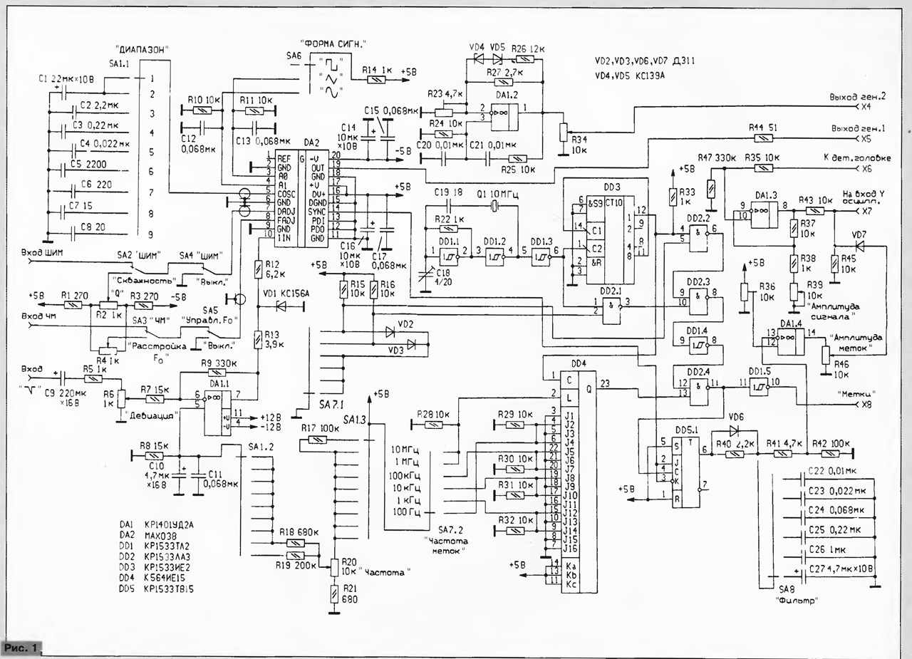
The basis of the generator (its scheme is shown in Fig. 1) chip is MUCH firm MAXIM, detailed description of which is given in [1].
(click to enlarge)
The deviation is in the lowermost according to the scheme position. The form of the output the signal generator is determined by the logic levels at the inputs AO, A1 and depends switch of SA6. It was observed the influence of instability of governors signals for the inputs AO and A1 for General instability of the oscillation frequency. For the purpose of to minimize this effect are the capacitors C12, C13, reducing the level of interference and ripple of the power supply.
The frequency of the generated signal depends on the capacitance CF connected to the output COSC (the capacitors C1 - C8) input voltage SADJ and flowing current to the input IIN. The sub-band selection is made by the switch SA1. Continuous adjustment of the frequency inside the sub-band occurs at the input IIN. The magnitude of the current supplied to entrance is determined by the resistance of the resistors R12, R13, gain Oh DA1.1 and the position of the slider of the variable resistor R 20. For sub-bands 2 - 8 she is 21…240 µa. When switching on the 9-th subband increases scale gain DA1.1 the reduction of OOS (introduction R19) and the magnitude of the current IIN increases to 160…750 μa. This is necessary because of the limitations of minimally permissible value of capacitance CF 20 pF. When switching to the first sub-range enter R17, reducing the voltage drop across R20, R21 ten times and reducing accordingly IIN to 2.1…24 mA.
Thus, for sub-bands 1 - 8 the overlap factor of 11 and when switching from one sub-band to another output frequency is changed to 10 time, so you can use one scaled scale smooth changes frequency. For the ninth range of individual scale, it is more distended, the overlap factor is about 4.7. For each specific instance DA2 better experimentally to choose the width of the ninth range of the boundary value generation frequency of the chip. In any case for expansion, contraction, or shift frequency bands can use the following formulas:
Fmin-UminR9/[CFR' ·(R12+R13)];
Fmax UmaxR9/[CFR' ·(R12+R13)],
where Umin= 5R21/(R20+R21), Umax= 5, R' = R18 - for subbands 1 to 8, R'= R19 - for sub-band 9; CF= C1 …C8 (for the corresponding sub-band).
The options presented in the formula are measured respectively: F - in kilohertz, U is in volts, R in ohms, C is in PF.
It should be noted that for the first subband due to the introduction of the resistor R17 the values Umin and Umax, is substituted in the formula for calculating the frequency, it is necessary reduce about ten times obtained. Capacitors C10, C11 designed to improve the stability constant of the control voltage, input 5 W DА1.1.
Relative frequency detuning (±50% of F0) is performed by the resistor R4 (SA3 in the "F0"). To obtain a frequency-modulated oscillations to the input of the FM serves external modulating signal and translate SA3 in upper circuit position (FM).
For pulse width modulation using the appropriate input of the PWM; adjusting the duty cycle produced by the resistor R2. The concept of "duty cycle" here applied somewhat arbitrarily, to be exact - is the change of the ratio of positive half concerning the length of period in percent: for rectangular hesitation it really is the duty cycle, but for the vibrations of a triangular shape is the ratio of time forward and reverse operation (signal change from "straight" saw to "return"), for a sinusoidal signal - change (distortion) of the form signal. The latter can be useful for minimizing harmonic distortion generator adjusting the shape of the sine wave.
The amplitude of the modulating signal inputs for FM and PWM should be not greater than ±2.3 V.
Switches SA4, SA5 designed to cut the duty cycle and management the frequency at inputs DADJ and FADJ circuits DA2, wherein the duty cycle is set equal to 2 (50 %), and the frequency exactly corresponds with resistor R20.
The output signal from the output OUT DA2 through a resistor R44 to the nest "Exit generator 1". Inputs COSC, DADJ, FADJ chips are very sensitive to external inductions, their connection to the switches is advisable to carry out screened cable or node generator positioned in a shielded compartment.
To regulate the output level of convenient to use outside attenuator, connected between the generator output and the input of the investigated device. Can you recommend an attenuator, is given in [2], it provides the attenuation range from 0 to 64 dB in 1 dB increments and is in good agreement with the input and the output impedance.
In the mode of oscillation frequency input " √ " generator connect with the corresponding the output of the oscilloscope. Control of the frequency sweep synchronously with scan oscilloscope is produced at the input of NN chips DA2. The signal from the input the capacitor C9, where the DC component is cut off. Further from the engine the variable resistor R6, which regulates the magnitude of the control signal and accordingly, the width of the swing of the generator is supplied to an inverting amplifier-adder DA1.1. Summed with a DC component, determines the center frequency of oscillation and adjustable resistor R20, the signal is input to the UN DA2. The Zener diode VD1 maximum allowable limits current to log IIN to the level of 750 mA.
Generator frequency tags consists of master oscillator on DD1.1 - DD1.3, dividers on DD3 and DD4, trigger DD5.1 and a comparator for DA1.4. Quartz the master oscillator generates a signal at 10 MHz, which is supplied to the input of the divider DD3 (a division ratio of 10). Further, from the output signal DD3 at 1 MHz is input to the divider with a variable division ratio of DD4. According switch of SA7.1 input With trigger DD5.1 will be present the signal frequency of 10 MHz, 1 MHz, or a signal whose frequency is determined the division ratio of DD4. The inputs of the JK-flip-flop is fed from the output of the SYNC DA2 the signal with frequency equal to the frequency of the output signal of the generator, and the phase shifted by 90 degrees. The trigger output is connected LPF on the elements R40, C22-S (the cutoff frequency is determined by the position SA8).
Thus, at the input of the comparator DA1.4 the resulting low-frequency beats the output frequency of the generator and frequencies that are multiples of the frequency of the clock input DD5.1. The amplitude of the beats is the higher, the closer for the above components the frequency axis. Therefore, when a smooth change of the output frequency signal generator input DA1.4 will be the signal bursts of the beating pointing to the multiplicity of the output frequency of the frequency generator signal labels. The width of the bursts (in time) depends on the bandwidth of the LPF and is determined the SA8 position, this is to get clear labels with different spans and on different ranges of the generator. Resistor R36 is determined by the threshold triggering of the comparator, cutting off the noise of the beating below a predetermined amplitude. The amplitude tags adjustable resistor R46 and added to the main signal at R45. The division ratio of DD4 is selected by the switch SA7.2 and allows you to get on the divider output signal with frequencies of 100, 10, 1 kHz, 100 Hz. When the situation in SA7 the two outer (upper circuit) the provisions DD4 produces a single account and stop - signal at its output Q no.
To extend the capabilities of the generator can be supplemented by the grid frequency signal labels required set of frequencies, for example 465 kHz, to configure the HRC radios. In this case, the division ratio is chosen according to the formula:
N = M (R+R+RS+ R4)+ R5,
where N is the division ratio; M - module defined by the code for Ka, KB, KC; P1 - multiplier thousand, determined by the code on J2, J3, J4; P2, PS, P4 - factorization of hundreds, tens, units, they are defined by the code J13-J16, J9 - J12, J5-J8; R5 - the remainder, which is determined by the code J1-J4.
Detailed description of the chip CIE given in [3]. The generator has separate output Tags, which can be useful in a number of dimensions, where you must have exemplary carcovado frequency.
Auxiliary generator frequency audio on DA1.2 is assembled according to the standard scheme, he can be used to modulate the main oscillator frequency or pulse width modulation or as a separate generator.
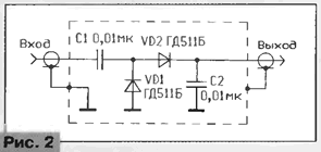
The detector (Fig. 2) is assembled by the voltage doubling circuit and allows you to work in the range of 10 kHz to 50 MHz using the frequency sweep of the oscilloscope is not more than 100 Hz.
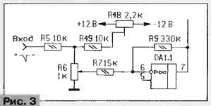
To study low-frequency circuits, the frequency sweep should to be very low, the use of a conventional oscilloscope allows you to see the frequency response. When available storage oscilloscope it is possible to observe the frequency characteristics, since the frequency of 0.1 Hz. Thus it is necessary to apply another input circuit synchronization, for example, shown in Fig. 3.
Also for this purpose it is better to make a separate detector head, increasing the capacitance of the capacitors C1 and C2 (see Fig. 2). The increase of their capacity expands the frequency range is from below, while reducing the allowable frequency sweep oscilloscope. To obtain labels at low frequencies it is necessary to choose corresponding to the division ratio of DD4 and instead filter on R40, C22-S apply high-q filter; limitation still exists - to highlight the beats at low frequencies difficult.
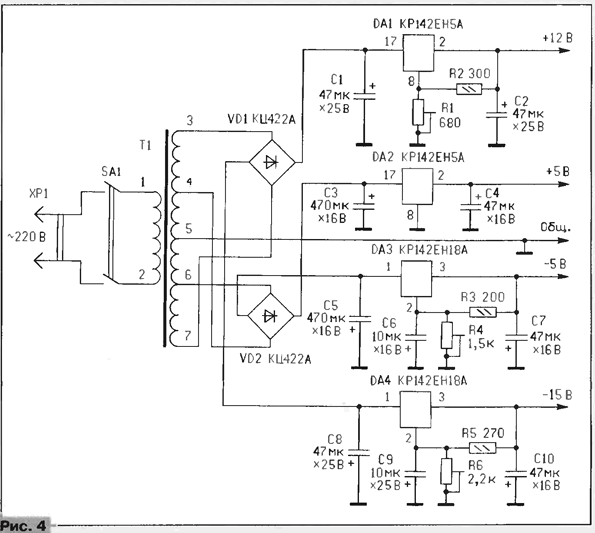
The power supply (Fig. 4) is assembled in the usual way and produces the supply voltage ±5 V and +12 V. the current consumption on the respective tires do not exceed specified limits: +5 V - 300 mA; -5 V - 100 mA;+12 V 50 mA; -12 V 50 mA.
In the device used resistors MLT 0,125, as the variables are allowed use a JV, SP, JS4. CustomNode capacitors must have low TKE - applicable KLS series, km-5 (C5-C8), K73-9, K73-16, K73-17 (C2-C4). Polar capacitor C1 - K52-1 low leakage current; the remaining capacitors - any. Switches SA1, SA6-SA8 - PG. Chip DD1 - DD3, DD5 interchangeable on similar series K155, K555, K, it is only necessary to consider the respective the change in the current consumption. Chip series 564 or C (DD4) it will replace CIE.
Printed circuit Board for the generator was not developed. When placing elements and connections on the Board it is necessary to separate as far as all circuits associated with inputs (pins 3-10) DA2 from the other circuits.
Tuning starts with the selection of the capacitors C1-C6, so that when the switching frequency ranges changed exactly ten times. Capacitors C7, C8 it is better to pick up after final Assembly design, as the total capacity of the CF for the sub-bands 8,9 affect the capacity of the connecting cable, installation and other parasitic capacitance.
After that graduate two scales for resistor R20 (for sub-bands 1 to 8 and 9). Next, check the output waveform depending on the situation SA6 and limits regulation of the duty cycle and the detuning. The range of adjustment can be changed, counting the divider R1-R4, bearing in mind that the voltages on the inputs and FADJ DADJ should be within ±2,3 V. Then the sign "√" signal from oscilloscope Y input of the oscilloscope connected to the output 7 DA1.1, the engine resistor R20 is set to the middle of one of the subbands, R6 put in upper circuit the position and the selection of R5 achieve that the signal at pin 7 DA1.1 was in the range 0,2…of 7.5 V. This corresponds to the maximum swing band. Inside the frequency bands may vary in 300 times, to reduce this value the resistance R5 is increased to the desired value.
Adjustment of the generator frequency tags begin with installation of frequency setpoint generator. A frequency counter connected to the output 6 DD1.3 and tunable capacitor C18 exhibit a frequency equal to 10 MHz. Next, verify that the frequencies on the output frequencies label the switch positions SA7. After that check the availability the beat signal at pin 13 DA1.4 and resistor R36 exhibit a threshold of the comparator to obtain a sharp narrow marks on the output DA1.4. In this setting the generator can be considered finished.
Auxiliary generator frequency audio on DA1.2 (see Fig. 1) configure adjusting R23 to obtain a stable generation of a sinusoidal signal.
Configuring the power supply is to put the relevant output voltages using resistors R1, R4, R6.
To study response collect the installation according to the scheme in Fig. 5.
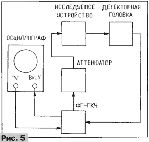
Switch SA6 translate to generate a sinusoidal signal. Estimated the location of the frequency response exhibited by the switch SA1 and the resistor R20, resistor R6 set the desired swing band (of the review). With the switch SA7 choose the desired frequency labels. Switch SA8 seek to the oscilloscope screen clear sustainable labels. By changing the parameters studied the device for track change feature points frequency response: frequency - regarding labels, amplitude - relative positions of the attenuator.
*Upper ninth frequency sub-band is determined by the specific instance chip MAH: its typical value is about 40 MHz, the minimum is 20 MHz.
Literature
Author: A. Malykin, Moscow