


")

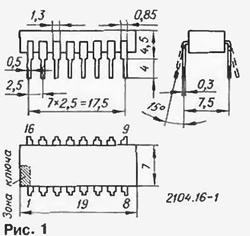
Chip CRES is intended for use in timers, time relays and as the pulse generator is low and subsonic frequencies. Chip is an RC oscillator and a controllable frequency divider with switchable division factor composed of several counters, switched feed high-level signals on the installation inputs. The maximum value the division factor is unique - 235 929 600. The chip is made by CMOS technology with samosbernymi gates of the transistors and the isolation of local oxide. Case - plastic 2104.16-1 (Fig. 1).
Weight - not more than 1.2 g .
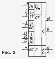
Scheme graphic symbol of the chip shown in Fig. 2.
The Pinout of the chip: pin. 1 - the input signal setting of division ratio of 26: pin. 2 - signal input reset; pin. 3 to the input of the stop signal counters; new. 4 - the amplifier-shaper, the output for connecting an RC circuit generator; pin. 5 - direct the output of the amplifier-shaper, the output for connection capacitor oscillator; pin. 6 - inverted output of the amplifier-shaper, the output to connect the resistor of the generator; pin. 7 - free; pin. 8 - General; negative power supply pin; pin. 9 - open-drain output of the frequency divider; pin. 10 - regular output of the frequency divider; high. 11 - signal input control phase the output signal from the pin. 9; pin. 12 - signal input factor setting unit division 60; pin. 13 - input setting of the division ratio of 3; pin. 14 - the input setting of the division ratio of 10; the pin. 15 - signal input setup the division ratio of 30; pin. 16 - positive power supply pin.
Main technical characteristics at Tamb. MS= -10.. .+70°C
- Nominal voltage, V......5
- Current consumption, mA, not more, at a voltage of 6 V mode static......20
- dynamic frequency 40 kHz......1000
- Output voltage low level, not more, at a voltage of 4 V, measured on the findings 5 and 6 (when the output current 1.6 mA)......0,4
- 9 (5,2 mA)......0,8
- Output high voltage, V, not less, at a voltage of 4 V and the output current is 1 mA, measured on the findings 5 and 6......3,6
- Input current low level, the ICA, not more, at a voltage of 6 V, measured in the output circuit 4......0.1
- Input current high-level mA, not more, at a voltage of 4 V. measured in circuit of the terminals 4 (at input voltage 4 In)......0,1
- 1-3, 11-15(6)......50
Limit operating values
- The voltage, V......4…6
- The maximum frequency of the clock pulses kHz......200
- Ambient temperature, °C......-10…+70
- Maximum static capacity, ......30
- Limit voltage of the power source for 10 seconds, In......10
- The total time of operation at extreme voltage for the entire period operation, h......1
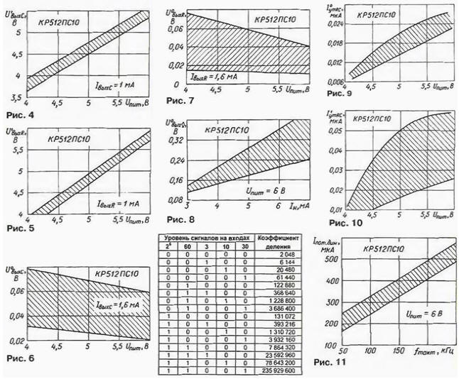
The division ratio of the frequency of the input signal current at pin 4 depends from the voltage levels on the installation inputs 26, 60, 3, 10. 30 (see the table). If all of these inputs served low logic level, the division ratio of is $ 211=2048. When applying a high level on a Ute or another installation log the specified coefficient should be multiplied by the weight value of the input. High level it is permissible to submit simultaneously to the inputs 26, 60 and one of the inputs 3, 10, 30. If high level to apply for two or three inputs from groups 3, 10, 30, will happen lock meter.
IN controls the phase of the signal at the output of the open drain. If the level is low this input signal at pin 9 of the anti-phase signal at pin 10, in high - in phase.
Supply high-level input R0 (zero) sets all counters-frequency dividers circuits in the zero state, corresponding a low level at pin 10. The operation begins with the receipt of this input low. High level input ST (stop) stops all counters at pin 10 remains the level that was before serving "Stop" signal. Counters resumes at the moment when this input comes low, since the state in which they were stopped. Submission of these signals does not stop the clock work generator.
In any division ratio of the output signal has a duty cycle of 2 ("meander"). The chip contains resistors that provide a logic low at all the inputs except the input RC. in the case when they are left free.
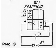
The structure of the chip allows to build a clock oscillator with external a resistor and a capacitor connected as shown in Fig. 3.
In Fig. 4 - 13 shows a typical dependence of the parameters on the voltage power, output current and frequency in an operating temperature range. The shaded region of variability for 95% of the chips. In Fig. 4 and 5 shows the dependence of the output voltage of high level at the outputs C and R respectively from the supply voltage, as in Fig. 6 and 7 is low.
In Fig. 8 shows a load characteristic of the open-drain output with the output voltage of low level. Fig. 9 and 10 illustrate the character the dependence of the leakage current input RC low and high input levels voltage respectively supply voltage.
Frequency dependence consumed in dynamic mode is shown in Fig. 11.
Author: S. Biryukov, Moscow