


")

In the experiments with complex, in particular a microprocessor, devices often require multi-channel, galvanically not associated power sources. The article describes the control device of a three-channel unit power supply with galvanically unrelated and randomly (according to polarity) plug-in sources. He has also the function of overload protection and electronic switch. You can disable all sources when overloading one of them. The device is electrically connected only to the source voltage +5 V, which is part of BP, from the rectifier which it feeds.
A schematic diagram of a control BP depicted in Fig. 1. It is three RS-triggers collected on the elements of DD2.1 and 2 DD2, DD2.3 and DD2.4, DD1.3 and DD1.4 with led lights HL1. HL2. HL3 accordingly, node matches the element DD3.3. start-stop devices made on the elements DD3.1, DD1.1, DD3.2, DD1.2. and parametric stabilizer the voltage at the transistor VT3 and the Zener diode VD4.
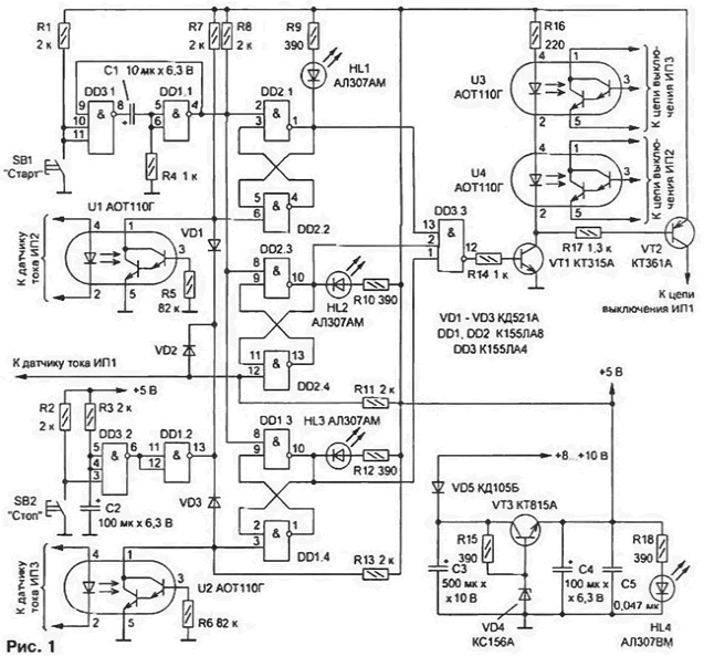
All trigger cells work the same way, so consider the work of one of them. for example, the gathered elements DD2.1 and DD2.2. When the power supply network switch the DC voltage from the rectifier output power supply +5 V (EP. not shown in the diagram) through the buffer diode VD5 is supplied to the stabilizer the voltage control device. The stabilized voltage +5 V through the resistor R3 is supplied to the inputs (pins 4. 5) item DD3.2 and condenser C2 jog device. As a result, the output DD3.2 momentum the voltage level of logic 1, and the output DD1.2 - level logic 0. Last through a decoupling diode VD1 is input (pin 6) item DD2.2 and sets the trigger DD2.1DD2.2 in the zero state (at pin 1 - the low level), which leads to the ignition of the led HL1.
A logic level 0 output DD2.1 is fed to pin 13 of the element matches DD3.3. This occurs when at its output a logic 1 opens transistors VT1 and VT2. and the led of optocoupler U3, U4 are lit. As a result open compound phototransistors, which are not allowed to join appropriate channels (IP2, forum) BP. Collector current VT2 off IP (+5). Transients in the flow control device faster than BP overall, therefore, the surge voltage at the outputs IP - forum is not observed.
To enable BP press the button SB1 ("Start"). On the elements of DD3.1 and DD1.1 assembled the single vibrator. generating the trigger pulse BP. approximately equal the duration of the half cycle of the network. This is necessary to limit the current short circuit or overload, the power through the elements of BP during the term of trigger pulse starts with overloaded PSU output. The negative pulse output from DD1.1 goes to pin 2 of the element DD2.1 and sets the trigger in one state. Thus HL1 led goes off, the logical 1 signal is supplied to pin 13 of the element matches DD3.3. and because voltage at other inputs (pins 1 and 2) have the same level, at its its output is a logic 0. As a result, the transistors VT1 and VT2 closed, the led of optocoupler U3 and U4 are extinguished and closed phototransistors include a PSU.
When there is overload in IP2 turn on the optocoupler U1. the phototransistor shunt input (pin 6) item DD2.2 and the trigger, which he is, set to the zero state. It is lit led HL1. on the output DD3.3 as a signal of logical 1 and, as a consequence, off sources of PD. Indicators HL2 and HL3 remain off, as the rest triggers remain in a single state. Thus there is led indication of channel PSU. in which there was an overload. After her eliminating unit include clicking on the button SB1.
Turn off the PSU button SB2 ("Stop"). The logic 0 signal arising from this output (pin 13) of the element DD1.2, sets all flip-flops in the device in the zero state, and LEDs HL1 - HL3 lit, signaling turn off the PSU. Led HL4 indicates presence of power to the device.
Transistors optocoupler U3. U4 is connected to the chains off IP2. Forum. LEDs optocoupler U1. U2 - with their current sensors, and the output element 12 DD2.4 - with sensor current IP (+5 V).
It is easy to see that the described device can easily be expanded to a desired the number of the control channels with the introduction of new triggers and replacing DD3.3 on the element with a large number of inputs. Also there is an opportunity to manage the work with BP other devices having output TTL levels. It is enough disable one of the inputs (pins 10. 11) item DD3.1 from the resistor R1, and one from the inputs (pins 4. 5) DD3.2 - from the resistor R3 and the capacitor C2 and connect them with chains of devices forming the logic 0 signals, respectively, for starting and turn off the PSU. Manual control is preserved.
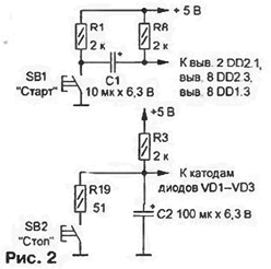
If the need for control from external devices do not. the device can be simplified by eliminating the elements of DD3.1, DD3.2. DD1.1. DD1.2 and resistor R4. Jog node in this case is collected by the diagrams shown in Fig. 2, and available the conclusions of the inputs of these elements connect the positive wire supply through a resistor R20 resistance 1 kω (new numbering resistors continues in Fig. 1).
The good parts, the device begins to work immediately and does not require adjustment. I the author for a long time it is operated as part of a three-channel laboratory BP. the voltage source +5 V which is the same as described in [1], and the other two identical and manufactured by a modified scheme published in [2] would to thank the author of [2] for a really good PSU circuitry.
Literature
Author: A. Muratov, Norilsk