


")

Homemade power supplies with pulse voltage stabilizers in the past times were very difficult to manufacture and set up, because they had produced entirely discrete. Therefore, in Amateur radio environment is much more popular with power supplies with linear the stabilizers.
The main shortcomings of the linear stabilizers are low Efficiency when the difference between input and output voltage, the need the use of a heat sink of considerable size, which entails an increase in the weight and dimensions of the structure. Device with a switched-mode regulator provide higher efficiency, lower weight and usually have smaller dimensions, comparing, with designs that use linear regulators voltage. Using specialized integrated circuits pulse stabilizers, it is possible to simplify the circuitry of the pulse stabilizers, while improving their reliability and performance characteristics.
A schematic diagram of a low power supply unit with a switched-mode regulator voltage is shown in Fig. 1. This power supply provides an output the voltage from 3.3 V to 9 V at load current up to 0.5 A. the switching regulator in this design is implemented on popular inexpensive integrated circuit, type MSAR company Motorola. This chip can operate under input voltage 3…40 In, allows you to create step-up step-up and inverting voltage converters. The chip included as pulse buck Converter. using it in this mode will be the most rational if the input voltage exceeds not stable less than 1.5 times. With less difference between the input and output voltage the efficiency of the stabilizer is reduced, approaching the efficiency of the linear stabilisers. The minimum difference between input and output voltage, necessary for normal operation of the downconverter is 3 V.
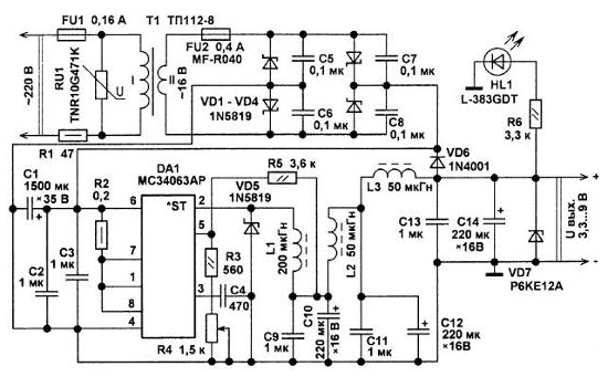
Fig. 1
Voltage AC 220 through the fuse FU1 and a non-combustible protective resistor R1 is supplied to the primary winding of the step-down the transformer T1. The voltage from the secondary winding of the transformer via resetable fuse FU2 is fed to a bridge rectifier, performed on Schottky diodes VD1…VD4. Capacitor C1 smoothes the ripple the rectified voltage. Varistor RU1 protects the mains transformer and diodes bridge rectifier from damage by surges in the line voltage and pulse interference.
The low-impedance resistor R2 is required to protect the IC from DA1 overload than greater the resistance, the less current is triggered, the built-in protection of the chip. The oscillator frequency of the chip is set by the capacitor C4. Schottky diode VD5 and storage choke L1 participate in the transformation of high input the low voltage output is stable, the value of which depends on the resistance of the resistor R5 and the total series resistance constant of the resistor R3 and the variable R4. Since the comparator chips strives to maintain at pin 5 voltage of approximately 1.25 V, then, the more the total resistance of the resistors R3 and R4, the smaller the output voltage the stabilizer. Inductors L2 and L3 are part of the LC filter, smoothing the stable output ripple voltage. Powerful Zener diode VD7 protects the load from damage in case of failure of the stabilizer, thus, work resetable fuse FU2. Diode VD6 reduces the likelihood of damage to the chip. HL1 led illuminates when the output the voltage regulator.
Accurately manufactured according to the scheme of Fig. 1 causing part of the power supply, not requires configuration of the power supply switching voltage DC performed on the popular IC series LM2575, the pulse voltage stabilizers performed on chips this the series is able to give to the load current up to 1 A. the Input voltage integral stabilizers series LM2575T can be up to 40 V. In this design applied chip type LM2575T-5.0, designed for fixed output the stabilized voltage +5 V. to widen the scope of application of the device with this stabilizer, used circuit solution to obtain and other voltages on the output of the PSU.
The node at the step-down transformer T1 operates as the same node in the first device. Capacitors C1, C2, C3 is the power supply filter circuits DA1. The inductor L1 is cumulative. Output voltage ripple stabilizer smooths two-tier low-pass filter C4C9L2C10C11L3 SS. The switch SB1 is possible to select the output voltage is 5 or 9 V. When open the contacts of this switch, the voltage on pin 4 DA1 is supplied through a resistor R2: resistance of which depends on the output voltage. Than more the resistance of this resistor, the higher the output voltage.
When the closed contacts SB1 output voltage of the stabilizer is equal to working voltage applied. It should be noted that lowering switching voltage regulators consume from the rectifier less current than given the current to the load. Moreover, the greater the difference between the input and the output voltage of the stabilizer, the lower the current will be at a constant the load current. For stable operation of the device, the capacitors C2, C3 must be installed as close as possible to the power pins of the chip DA1. This condition is also it is desirable to perform and to capacitor C1.
In Fig. 2. a diagram of a more powerful chip, in this case, 5,2 5,0…V.
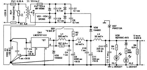
Fig. 2
The resistor R3 and the diode VD6 reduce the likelihood of damage to the chip.
When the output voltage of 5 V is lit green led HL1. At an output a voltage of 9 V will Shine and the red led HL2, since the voltage at the output of the regulator will be more than the total operating voltage of the led HL2 and the Zener diode VD8. Powerful Zener diode VD7 mounted on the output the voltage regulator reduces the likelihood of damage to the load when failure the stabilizer.
Unmistakably made of non-defective parts according to the scheme of Fig. 2 power pack starts to work immediately after switching on the network. If necessary, the selection resistor R2 can be precisely set the output voltage 9 V or another close to it, which you will need. In the place of R2 can be installed and variable resistor, then, there will be a smooth regulation of the output voltage, for example, from 5 to 12 V. Metal the case is the screen of the variable resistor should be connected to GND.
When the output voltage of the stabilizer 9 In, load current of 1 A, the input voltage 16 In consumed current stabilizer will be about 0.6 A, which corresponds to its Efficiency is about 93% excluding losses in the step-down transformer and bridge the rectifier. For comparison, the efficiency of the linear regulator under the same conditions would be no more than 56%. When the input voltage is 19 V, output 5 V DC load 1 And consumed by the stabilizer from the bridge rectifier current will be around 0.31, which corresponds to an efficiency of about 84%, the amplitude of the voltage ripple at the output of the regulator at the maximum load current does not exceed 20 mV the frequency of operation of the pulse Converter DA1.
In Fig. 3 is a schematic diagram of a more powerful power source that represents charger-power supply device with pulse voltage stabilizer. This device allows you to connect to yourself simultaneously two devices, such as pocket Flash player, camera, mobile phone to recharge their batteries through interface USB cable or directly to power these devices for the purpose conserve battery resources. In addition, this design can be used as a powerful laboratory power supply with overload protection. The device is assembled with the use of an integrated circuit company SGS-Thomson Microelectronics type L4960, representing the adjustable step-down switching regulator voltage. This chip is able to provide the current in the load up to 2.5 A, it output voltage +5.40 In, up to 90% efficiency. The maximum voltage chip L4960 +46 V. the Chip has a built-in overload protection and overheating.
The node at the step-down transformer T1 operates as the same node in the earlier devices. The rectified voltage ripple smoothing oxide high-capacity condenser C4. The DC voltage is supplied integrated switching regulator DA1. In Fig. 3 shows a schematic the scheme is even more powerful power supply.
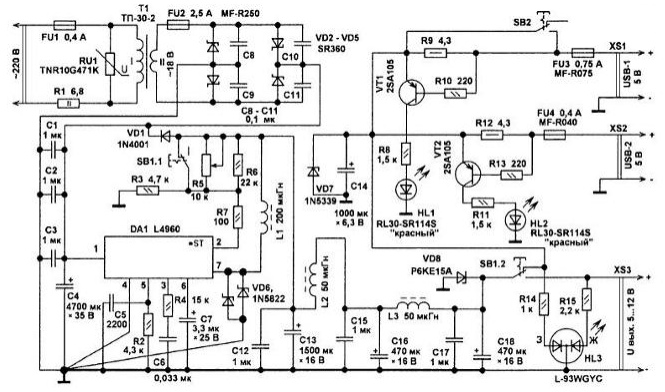
Fig. 3
Conversion frequency DA1 about 83 kHz with a load current of 1 A. the Inductor L1 -cumulative. The output voltage depends on the ratio of the resistances resistors R5, R6 and R3. At zero the total resistance of the variable resistor R5 and resistor R6, the output voltage of the switching regulator can be 5,2 5,0…V. output voltage Ripple smoothing two-element LC N-filter SS L2C15С16L3C17С18. Output voltage ripple does not exceed 20 mV the frequency of operation of the Converter when the load current of 1 A. the Resistor R7 and the diode VD1 protect DA1 from possible damage.
This power supply can operate in two modes, selectable button SB1 In the position shown in the schematic diagram, the device operates as a USB charger with output voltage +5 V, which does not depend on the position of the engine variable resistor R5. If SB1 translate into a second position, the device will work as a power supply with adjustable output voltage. The mode is indicated by led HL3. When working in design mode "Charger" this led shines green or yellow green when the device operates as a laboratory power supply. Nodes on transistors VT1, VT2 are intended to indicate the presence of the charging current. When specified in the concept the resistance of the resistors R9, R12 LEDs HL1, HL2 Shine when the current flows through the corresponding load more than 150 mA. If you the LEDs will Shine at a lower charging current, silicon transistors 2SA105 can be replaced by germanium, for example, NB. MPA, MP that preferably, install the resistors R9, R12 at a higher resistance. Resettable fuses FU3, FU4 triggered by short circuit or overload condition. Powerful Zener diode VD7 and capacitor C14 protects connected to the USB sockets of the device from the burst output voltage, which can occur when you switch SB1.
You should pay attention that the power to the socket XS1 is fed through a more high current resettable fuse FU3. Furthermore, the presence of button SB2 allows you to connect to this socket device with a relatively large the current consumption. For this purpose the contacts SB2 should be closed, which excludes the fall of the output voltage across the resistor R9. Powerful Zener diode VD8 reduces the likelihood of damage to the load when the malfunction of the voltage regulator. If for some reason the output voltage of the stabilizer will be more than 15 In, or work built-in protection circuits, or resetable fuse FU2. If the power supply is turned off as soon as time, the Zener diode VD8 is broken. To avoid the breakdown of the protective the Zener diode in this and previous designs, surge protection can to complement the standard trinistorny node consisting of a single average SCR the power of one Zener diode and one resistor.
Instead of a step-down transformer. TP-8 will fit any size and capacity 7 W and a voltage at the secondary winding 14…18 V. Instead of the transformer type. TP-7 will fit any with an overall capacity of not less than 13 watts and voltage the secondary winding 15.20 V. Transformer type. TP-30-2 can be replaced. HTTP or similar with an overall capacity of not less than 30 watts. The higher the output voltage of the rectifier bridge, the less current it consumes stabilizer, constant voltage load. The varistor can be replaced TNR10G471K any 430, 470, for example, FNR-C, FNR-14K471 MLT, S1-4, S2-23 S1-14. The resistor R1 in all schemes it is desirable to use a non-combustible, for example. P1-7 wire or small power 1 or 2 watts ceramic housing. Variable resistor - SDR-4 or equivalent linear characteristic. On the axis of the variable resistor is necessary to put on the handle of the insulating material.
Oxide capacitors - import analogues C50-35, K50-68, K53-19. Nonpolar capacitors - ceramic, imported analogues K10-17, km-5, km-6 or bezvyhodnuyu in SMD version. Ceramic capacitors installed parallel diode bridge rectifier and the input voltage stabilizers should be on the operating voltage of not less than 30 V. the Remaining ceramic capacitors can be installed on the operating voltage of 16 V.
Instead of Schottky diodes SR360 you can apply diodes MBR350, 1N5825, MBR360, DQ06, MBRD660CT, MBR1060, 50WR06. These diodes can be replaced 1N5822 Schottky diodes and low-power diodes Schottky - 1N5819, In the absence of diodes with Schottky barrier instead, you can use diodes series CD, D Instead of 1n4001 diode can apply any of the series part no 1n4001 -1N4007, UF4001 - UFN4007, CD, CD, CD. A Zener diode can CSA replace XV. 1N5341. Zener 1N5339 can be replaced by RMTCS. 1SMB5919BT3, 1N5919. Zener diode BZV55C-4V3 can be replaced by 1N4731A, TZMC-4V3 Instead of the Zener diode. RCEA you can install 1N5349 or DD. Instead of the Zener diode. RCEA fit 1 N5352, DE. The LEDs will fit any similar continuous emission color. Instead of p-n-p low-power transistors 2SA105 will fit any of the series SS9015, 2SA542, KT361, CT, CT CT.
An integrated circuit MSAR can be replaced by MSAR or more reliable MSA, made in the case DIP-8. To improve the reliability on such chips with thermally conductive glue stick copper finned heatsink cooling surface area of 8 cm square integrated circuit LM2575T-5.0 is designed for output voltage +5 V, made in petitioner the body of THE to-220 Instead you can apply chip LM2575TV-5.0. made in the housing. THE to-220 or L. M2575D2T-5.0, or similar chip from the LM2576. Chip LM2576 series allow a load current up to 3 A. Among chip series LM2575, LM2576 there are also chips in fixed output voltages of 3.3 V, 12 V, 15 V, and adjustable - Adj the output voltage 1,23…37 V. the Chip must be installed on copper or duralumin heatsink area a cooling surface at least 60 cm square If the PSU is assembled on the Fig. 2, will be designed for a load current of 3 A, the heat sink for chip series LM2576 must be at least 200 cm square and in close poorly ventilated housing is not less than 300 cm square Chip L4960 must also be installed on a heat sink with the cooling surface area of not less than 200 cm square (one side).
Instead polymer resettable fuses MF series-R fit similar LP60 series. Type switches. P2K, SDH, free group contacts which are connected in parallel. Storage choke (L1 all schemes) should be inductance 150.300 µh, can be manufactured in an annular magnetic core Chg ferrite NN. In the ring the diamond disk a saw or a good hacksaw is done through a slit width of 1…1.5 mm. In the crack glued a piece of PCB with foil. After winding ring varnished cloth, a Litz wire 22x0,18 mm coil 50…60 turns, it will be about 2 meters of wire. If the manufacture of the cut ring will break on the two halves can be glued instant superglue.
Between the winding layers need to lay one layer of varnished cloth or. PVC electrical tape. Each layer winding is impregnated with napolcom. Inductors L2 and L3 in all schemes contain 15 turns of the same wire, wound on a ring CHH ferrite MNM. Before laying the winding ring a bit nadpilivayut and broken into two the halves. Then glue instant glue or adhesive. BF and dry at least one day at room temperature. For stabilizer voltage is the scheme of Fig. 1, it is possible to apply a magnetic smaller size. You can apply also suitable chokes industrial manufacturing, with the resistance of the windings is not more than 0.05 Ohms. For stabilizer, assembled according to the diagram of Fig. 3, it is desirable that the resistance of the windings of the choke it was not more than 0.02 Ohms. In addition, in place of the inductors L2 and L3 can be applied chokes made on. The h-shaped ferrite cores, for example, from coils correction CRT TVs and monitors.
Author: A. L. Butov