


")

A regulated power supply is an integral part of Amateur radio lab. In the magazine "Radio" was described many such devices, however, some of they have low efficiency. The fact that most laboratory power supply made on the basis of linear stabilizers as to eliminate the main the lack of pulse sources of elevated levels of pulsation is often very difficult. As a rule, the consequence of such circuit solutions - increased loss of power. The author proposes his solution to this problem.
To increase the efficiency of the stabilizer to make it dostupnym: the first stage - pulsed preliminary stabilizer; the other is an ordinary linear. Both stages involved in feedback, so that the linear stabilizer supported minimum allowable voltage drop and thereby ensures high efficiency.
The switching regulator collected on modern element base [1, 2], high operational settings, including small losses. These the devices were used as a basis for the development of the proposed laboratory block power.
Main technical characteristics
- Input voltage, V......43
- The interval of the output voltage, ......0…35
- The maximum load current, And......7,5
- Conversion frequency switching regulator, kHz......55
Diagram of the device shown in Fig. 1. Switching regulator first stage assembled on a chip CHI-controller TL598 (DA4) by Texas Instruments, which controls the switching transistor IRF9540 (VT3). Chip differs TL598 from common TL494 by the presence of the output push-pull amplifier (nearest the characteristics of the domestic SHI-controller - CREW). Used this chip due to its high technical parameters: output current up to 0.2 A, a clock frequency up to 300 kHz, and a small price.
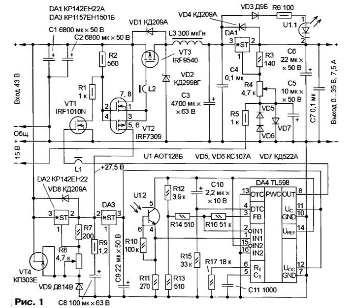
The use of a switching field-effect transistor IRF9540 (VT3) and a diode of a Schottky KDG (VD2) with a small voltage drop and recovery time allowed to increase the efficiency of the switching regulator to about 90 %. To increase throttle limits the output voltage of the buffer amplifier transistor the Assembly VT2 is fed from the auxiliary stabilizer on the chip DA2. Parametric voltage regulator FET and VT4 the Zener diode VD9 improves the stabilization factor and allows you to work at a larger input voltage. Resistor R9 in the circuit filter capacitor C8 protects the chip from DA2 overload at the moment of switching devices.
From the output of the switching regulator voltage is supplied to the linear stabilizer, assembled on a chip DA1 with a low voltage drop. In this circuit design, the output characteristics of the laboratory unit is determined parameters of the chip, which provides good attenuation of pulsations, the overcurrent and overheating and loss of power it is approximately equal to 5 %.
To the output voltage of the unit to adjust the zero, the circuit control output circuits DA1 served voltage 15V from a separate source.
Transistor optocoupler U1 maintains the voltage drop across the linear the stabilizer is about 1.5 V. If the voltage drop on the chip increases (for example, due to the increase of the input voltage), radiant the diode of the optocoupler and, accordingly, the phototransistor open. CHI-controller off, closing the switching transistor. The input voltage of the linear the stabilizer is reduced.
To increase the stability of the resistor R3 is placed as close as possible to the chip stabilizer DA1.
Inductors L1, L2 are ferrite segments of tubes mounted on the findings of the field gates transistors VT1, VT3. The length of these tubes is approximately equal to half the length of the output.
The inductor L3 is wound on two stacked annular magnetic cores CHH,5 of permalloy MP. Its winding contains 45 of turns wound in two of PEV-2 1 mm diameter, arranged evenly around the perimeter of the magnetic circuit.
Since the load current is close to maximum on the stabilizer DA1 and the transistor VT3 is allocated considerable power, they should be installed on the sinks area of not less than 30 cm2. Transistor IRF9540 (VT3) valid replace IRF4905, and the transistor IRF1010N (VT1) - BUZ11, IRF540, KB.
The area of the heat sinks is calculated according to the method described in [3].
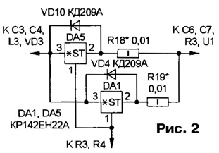
If you need a unit with an output current exceeding 7.5 A, you must add another stabilizer DA5 parallel DA1 (Fig. 2). Then the maximum current the load will reach 15 A. In this case, the inductor L3 is wound bundle comprising of the four wires sew-2 with a diameter of 1 mm, and increase about two times the capacitance of the capacitors C1 - C3. Resistors R18, R19 are selected by the same degree heating circuits DA1, DA5. CHI-controller must be replaced by another, allowing work at a higher frequency, for example, CREW.
If necessary, a large load current no, the stabilizer can CREA replace CRON (maximum current of 5 A or CREA(1.5 A).
Literature
Author: S. Korenev, Krasnoyarsk