


")

In recent years, the stores have a large number of simple telephones foreign production, to which there is no technical documentation. The author proposes a scheme and recommendations for repair of the two models telephones - VTM and VTR.
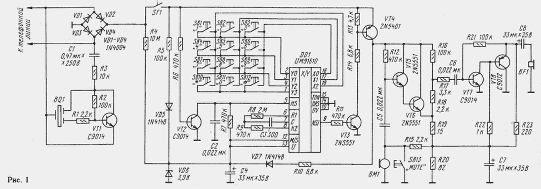
In the repair process of each telephone set (TA) have to study it the principle of operation. Consider first the model BT60M. The layout of this phone shows in Fig. 1.
(click to enlarge)
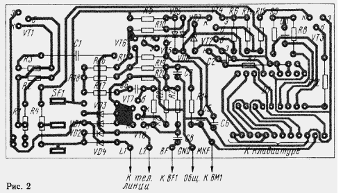
Lever switch SF1 shown in the diagram in the "tube put". SHE collected two printed circuit boards - basic (Fig. 2) Board and the keyboard, which are interconnected by a belt loop.
In this device were found the following defects: when dialing auditioned impulses, but in the line set is not worked out; when talking the person on the other end complained about the low level audio of the signal.
In the process of repair was found that faulty transistor VT3 role pulse key, and was leaking collector-emitter of the transistor VT5. After replacing these transistors phone began to work normally.
Chip UM91610A can be replaced by VT91611.
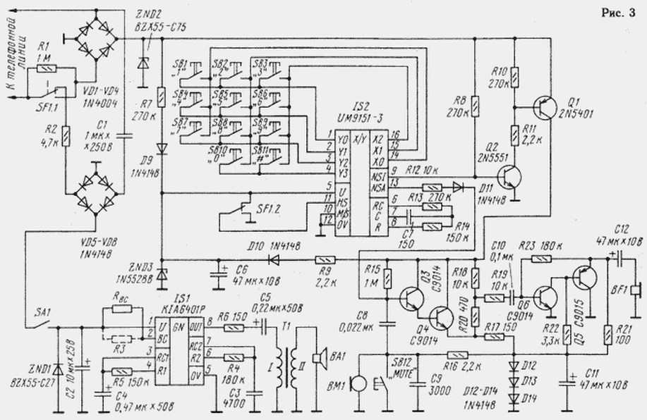
In Fig. 3 shows a diagram of the phone models BT960P. Lever switch SF1 shown in the "on-hook". Chips instead of IS2 (UM9151-3) suitable CRUZ or FT9151-3 with the corresponding selection circuits oscillator. On the chip IS1 (also suitable CROP or FT2410) assembled generator ringing signal.
(click to enlarge)
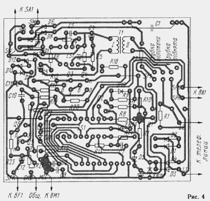
During the repair of the device were found such fault: not working calling device, when the conversation was hard to hear on the other end the telephone line. The transistor Q2 has been broken. On the main Board (Fig. 4) there was no resistor R3, shown dashed, although the seat for him there. When repairing the calling device revealed that the resistor R3 establish in the event when using the chip CA.
There are two groups of chips for calling devices. In the first group of resistor RВС(R3) connected between the input VS and GND, allows you to force to disable the generation at power supply voltage of the chip, equal to the working (25,1…of 28.9 In). This group includes the following chips: CRAP, FT2410, CA, ML8204, DBL5001 etc Type used depends on the Zener diode the operating voltage of the chip [1].
In the second resistor group RВС(R3) connected between the input sun and the housing, allows you to change the input impedance of the chip [2]. This group includes chip CRAP, FT2410, CA, ML8205, DBL5002.
As installed in this phone chip belongs to the first group, the R3 resistor should have a resistance of 220 ohms (with an operating voltage of 27 V) and it should be connected between the first (U) and second (CS) pins IS1.
Chip calling devices of the first and second groups on technical parameters the same, but the control input (VS) for each group performs its functions. Detail on these chips can be found in [2].
Literature
Author: S. Derevyanko, Cherkessk