


")

TV SIESTA model J-3128, the appearance of which is shown in Fig. 1, - portable TV black and white image with a screen size diagonally 31 cm and a remote control. There is provided a switching power supply AC 220 (±10%) or 110 (+10%) To and from an external source DC voltage of 12.6 V (±20%). Consumption power from the network is about 30 W, and from an independent source - not more than 18 watts.
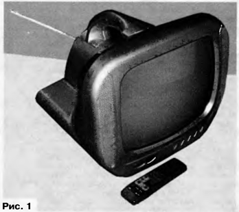
The sensitivity of the tract, the picture on the TV, limited synchronization, in the range of meter waves (MB) is no worse (no more than) 40 mV, in the range decimeter waves (UHF) - not worse (not more than) 70 mV. Nominal output channel power audio equal to 1 watt. Dimensions (width x height x depth) of the TV - 330x255x385 mm.
The kit includes TV indoor antenna and remote control (The remote control). The remote can control the device at a distance of 5 m.
Turn the TV on with the button mounted on the face panel. And clicking switch on the network causes an operating mode of the apparatus. Buttons "P+" or "P-" to switch programs, then press "V+" and "V -" to adjust the volume of sound.
The remote control contains a number of controls and settings of the TV. Any of the digital buttons to switch programs. Buttons "P+" and "R-" remote control switch program sequentially around the ring. Click "V+" and "V-" provide volume control sound, and the icon button in the form crisscrossed the dynamic of her head you can turn off and press again to re-enable. The "Menu" button calls the operation of the TV settings and press "AC off" turn it off.
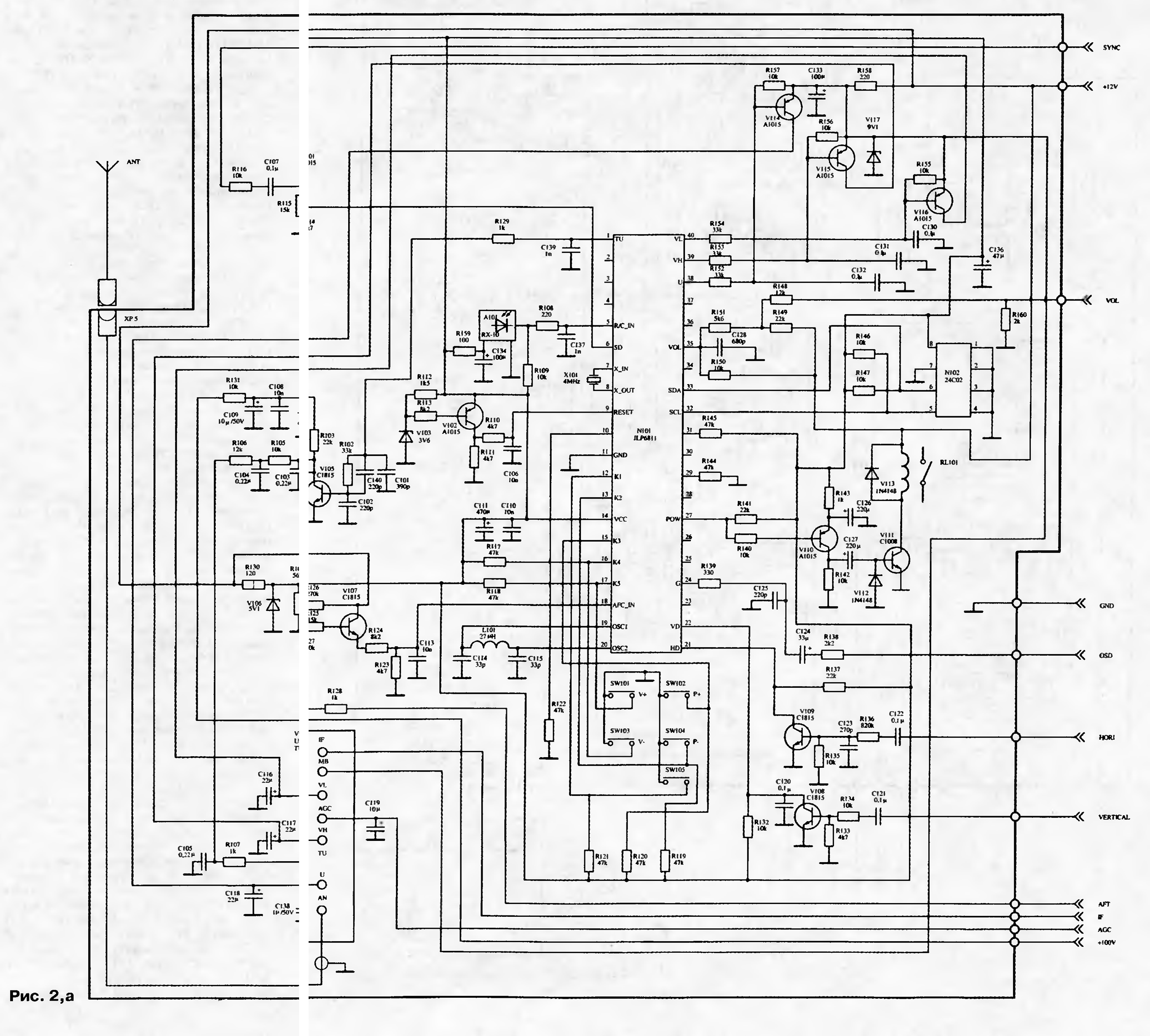
Schematic diagram of the TV are represented in Fig. 2. It utilizes the photodetector A101 infrared (IR) radiation from the remote control. Adopted signal through Low-pass filter R108С137 is fed to the input (pin 5) N101 chip, the first of five used in the TV chip company NEC.
(click to enlarge)
(click to enlarge)
Chip N101 as instruction decoder control is a microprocessor with specialized ports. Each port performs a separate function control TV, forming the corresponding signals.
Team "AC off" leads to the appearance at pin 27 of the microprocessor pulse negative polarity through resistor R140 opens the transistor V110. When the capacitor C is charged through the emitter junction of transistor V111, opening it to saturation. The collector current of the transistor flowing through the coil included in the circuit of the solenoid RL101, causing it to trigger and disable network TV power.
With the control buttons SW101 - SW105, located on the front panel of the TV, commands come through the terminals 12, 13, 15-17 microprocessor on the relevant ports. The result is a switching programs in direct (on ascending order of the numbers) press "P+" and reverse button "R-" order management volume to increase press "V+" or decrease button "V" it level, and also control the TV setting the "Menu"button.
Through the outlet 24, the low pass filter R139С125 and chain C124R138 signal forming on the screen graphic images of executed commands (OSD), is fed to transistor base V501 amplifier. Logic levels from the terminals 38 and 40 of the microprocessor through the corresponding low-pass filters R152C132, R153C131 and R154C130 control transistors V114-V116 respectively. Through these transistors required voltage for the inclusion of sub-bands arrive at the relevant conclusions of the channel selector.
To ensure synchronization on the display of information on pins 21 and 22 microprocessor filed lowercase and human impulses, respectively, taken from the output stages of the scan. The amplitude and polarity of the row pulse is determined by the elements S, R136, S, R135 and cascade transistor V109, and the amplitude and polarity of human impulses - elements S, R134, R133, and S cascade transistor V108.
Identification signal synchronization required for auto-tuning a television program is supplied to pin 6 of the microprocessor with cascade on the transistor V101. He forms it from the clock, remove from the selector clock transistor V401.
For internal generators connected to the microprocessor quartz the resonator H frequency of 4 MHz (findings 7, 8) and U-shaped filter C114C115L101 (findings 19, 20).
Pin 9 of the microprocessor is designed to reset the counter programs and setting zero addresses. When applying the voltage +5 V transistor V102 is opened and the capacitor C begins to charge through resistor R110. However, in the initial moment the voltage on the capacitor equal to 0 and the duration of its action depends on the time constant of charging of the capacitor. This level the counter is reset programs. After charging the capacitor to a level 1 the microprocessor will begin to operate in accordance with a program ROM.
The volume control and the TV setting is provided by the formation of the outputs of the corresponding ports signals with pulse-width modulation (PWM). With output 35 of the microprocessor PWM signal control volume is converted chain
C128R150 in the voltage adjusting volume. Through the divider R149R151 and low-pass filter R148R160C302 it affects the pin 14 of the chip N301.
With pin 1 of the microprocessor PWM signal configuration management formed capacitor C and sharpening chain R129C101R102C140C102 comes to base transistor V105. With his header after passing the four-bar RC-circuit R104 - R107C103 - SS it is converted to a voltage configuration management the channel selector. The voltage at the transistor V105 fed through a resistor R103 with a stabilized source to the Zener diode V104, through which resistor R131 comes a voltage amplifier with a capacitor C.
To store information about settings for a long time even when no supply voltage applied in the TV nonvolatile programmable read only memory - a chip N102, connected to the microprocessor via terminals 32, 33.
In all-wave TV set uses the channel selector of the production of one of countries in Southeast Asia that would enable the reception of broadcast television channels in the range of MB (VHF) and UHF (UHF).
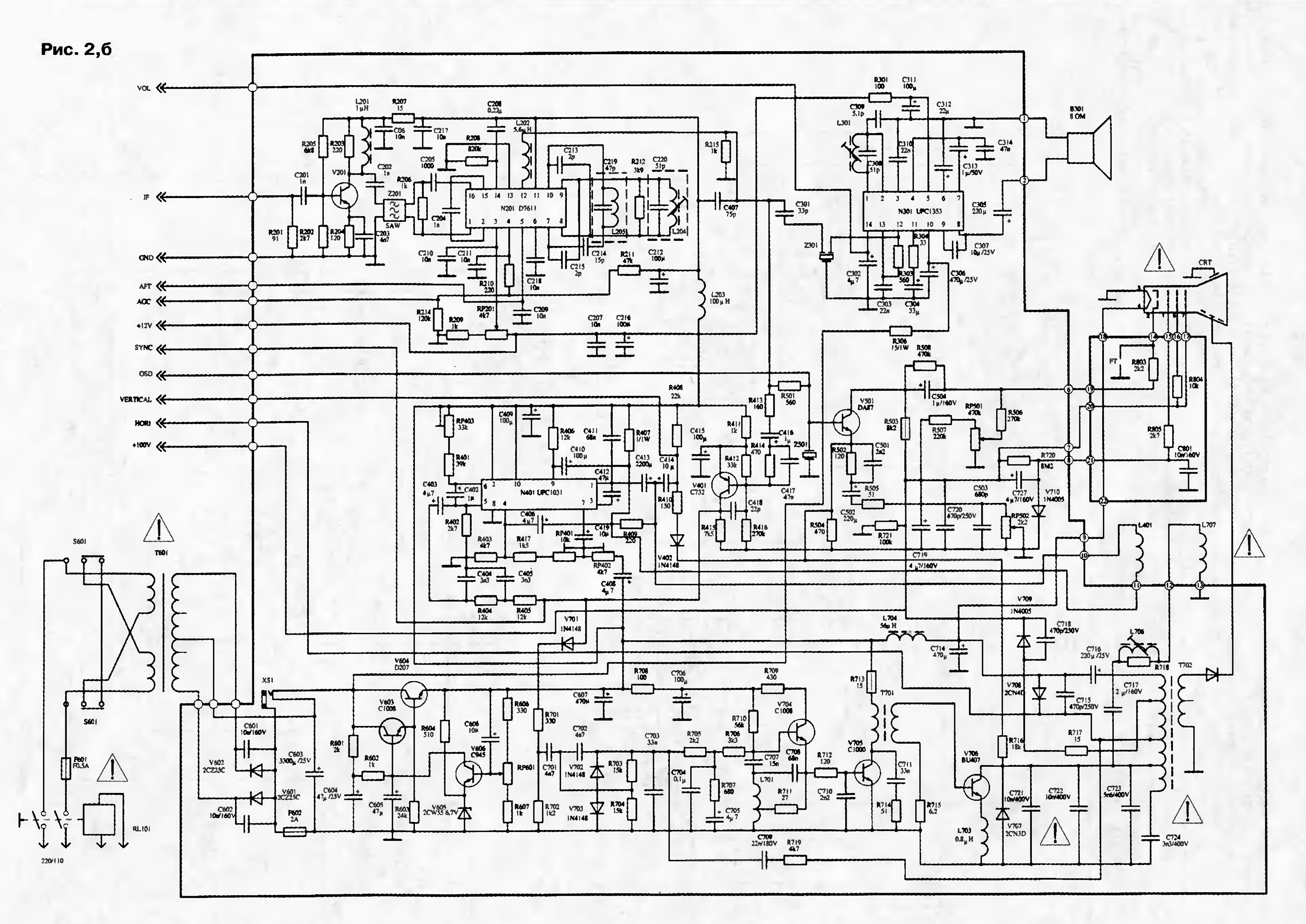
Adopted by the antenna of the radio signals passing through the channel selector is converted to signal intermediate frequency (if). This if signal from the output of the IF selector via capacitor C arrives at the pre-if amplifier, assembled on the transistor V201. Its input impedance mode provides matching with the output of the channel selector in the band FC. Pre-amplifier compensates the attenuation of the if signal, following the saw filter Z201. The filter forms Frequency response of if amplifier image (UPCI) with the set norms of attenuation in the band suppression of spurious signals and the required bandwidth of the if signal. The advantages of such filters can be called stability frequency response in the passband UPCI and their repeatability in manufacturing.
The main gain of the frequencies occurs in the chip N201, which contains the main UPCI, videogamemaster, operating in the synchronous detection (DM), the demodulator DM signal automatic frequency local oscillator (APCG) with amplifier DC voltage error, pre-amplifier and the automatic gain control (AGC).
The if signal passes through pins 1, 16 in the chip increases in UPCI and is being detected videogamecentral. Inside the chip the received video signal comes pre-amplifier.
Mode phase relations in the works of videodermatoscopy DM is set to the first exemplary circuit L204C220R212 connected to the terminals 8 and 9 of the chip N201. Second exemplary circuit L205C219C213-S connected to the terminals 7, 10 circuits N201, provides the phase relationship of the demodulator DM system APCG. In it the frequency of the if signal is compared with the frequency of the reference circuit and produces an error voltage proportional to the difference of these frequencies. The value and sign of the voltage error determined by the frequency deviation of the local oscillator in the channel selector from nominal. System APCG supports the frequency of the local oscillator the channel selector with the precision determined by the residual detuning in the loop regulation. To change the lo frequency to the value of the residual mismatch is an error voltage from the output of the DC amplifier through the output terminal 5 chip N201 and chain C209R128 is supplied to the emitter follower at the transistor V107, from which it passes to a microprocessor N101 (conclusion 18). In the microprocessor, the error voltage is summed with the voltage setting channel selector mode signal PWM, acting on the output 1 of the microprocessor.
The video signal inside the chip N201 also comes on the device ARU, which has two outputs. Through one on-chip AGC voltage affects the main UPCI. The latter is a three-stage differential amplifier with adjustable emitter feedback circuit which provides basic direct gain control of the channel image.
On another output (pin 4 of the chip) devices ARU is formed voltage control the gain of the channel selector. It through the filter R210C119 comes on selector. The AGC voltage on it, unlike the AGC voltage main UPCI, acts in a delayed mode, wherein the gain control selector starts with some level of RF signal at its antenna input. The delay install through the terminal 3 chip N201 voltage from the AC engine resistor RP201. The time constant of AGC set chain R208C208 via pin 14 chip.
Reinforced composite video containing the actual video sync pulse and the signal of the second inverter of the sound is obtained at pin 12 of the chip N201. Through a chain of RF correction L202R215C407, resistor R501 and notch piezoceramic filter Z501, which suppresses the signals of the second inverter of the sound, he does to the base of transistor V501 output amplifier with elements of RF correction R502, S, R505, S503. The voltage amplifier is formed by rectifying the pulses taken from the flyback transformer through T resistor R717, diode and V709 capacitor S. Load amplifier - the resistor R503. Through a chain C504R508 and resistor R803 the video comes on the cathode of the kinescope.
Variable resistor RP502 included in the emitter circuit of the feedback amplifier R502C501 - C503R505RP502, you can change the gain of the stage, i.e. the contrast of the image. Brightness adjust variable resistor RP501. With it engine power is drawn through the resistor R506 to the cathode of a kinescope, asking him mode DC. For blanking the beam during the return stroke vertical and horizontally on the emitter of the transistor V501 filed personnel (through the capacitor S, resistor R410 and diode V402) and lowercase (through a resistor R716) positive pulses covering the transistor.
From the complete video signal which has passed through the coupling capacitor C301, piezoceramic filter Z301 extracts a signal of the second inverter of sound through the terminals 12 and 13 of the chip N301 comes to being in it the amplifier-limiter. Besides him, the chip comprises a demodulator DM sound signal FM, electronic volume control and amplifier.
In the demodulator, the if signal of the sound coming from the amplifier-limiter, detected, resulting in a signal 3H. Providing a phase the ratio of operation of the exemplary demodulator circuit connected via L301C308 pins 1 and 2 of the chip. Inside the 3H signal passes through electronic the volume control, and then through the capacitor C313 included between pins 4 and 7, is connected to a power amplifier. Volume control is electronic method - enable pin 14 of the chip constant voltage regulating.
From pin 8 of the chip N301 through the coupling capacitor C305 reinforced the 3H signal comes to the dynamic head V with a nominal impedance of 8 Ohm. Through pin 6 of the chip power amplifier connected decoupling the capacitor C312, pin 9 - corrective feedback capacitor C307.
Full video through a chain R413C416R414C417 submitted also to the base of transistor V401 , which aggregates the selector clock. Transistor mode is selected so that it only opens word clock, which stand out on its load - resistor R415.
To highlight the human clock is enabled dvuhsvetnyj the low pass filter R405C405R404C404, which are filtered lowercase sync. Dedicated HR clock is input through a capacitor C and pin 5 of the chip N401 synchronize the generator human impulses, nahodyaschiysya in the chip. In addition, it contains a sawtooth generator and output stage frame scanning. Specifies the circuit of the generator human impulses are formed elements RP403, R401, S and connected to the terminals 5 and 6 of the chip. Trimmer RP403 establish the required frequency of HR sweep.
Formed human impulses inside the chip sync generator the sawtooth voltage. Through the terminals 4 and 7 of chip resistors R417, PR401, capacitor C sawtooth voltage is supplied to the output stage personnel sweep. Trimmer RP401 change the size of the image vertical and trimmer RP402 within the chain C408RP402, - the linearity.
Amplified in the output stage human impulses through pin 1 of the chip and N401 coupling capacitor C come on HR coil L401 deflecting system (OS) of the kinescope. The feedback signal through the capacitor C and conclusion 3 chip goes to the output stage.
Elements R406, S, is connected to pin 9 of the chip, and the capacitor C, is connected to pin 4, provide feedback to cascade HR sweep, stabilizing the image size vertically.
Flyback pulses from the collector of transistor V401 through the chain V701R701R702C701 pass to the phase detector device PLL (phase automatic frequency control), harvested diodes V702, V703. With the flyback transformer T through the chain R719C709 to the phase detector filed flyback flyback pulses which are integrated by the capacitor C. With the device PLL regulating the voltage across the filter R705C704R707C705 and resistor R706 is supplied to the base of transistor V704 specifies the blocking oscillator lowercase sweep.
Feature applied linear master oscillator is very stable work that does not require adjustment of the frequency lines.
In the emitter circuit of the transistor V704 produced lowercase triggering pulses, which through a chain R712C710 come to the base of transistor V705 grooms cascade horizontal. In the collector circuit of the transistor included primary winding of the matching transformer T. Pulses with its secondary winding control the emitter junction of transistor V706 horizontal output stage sweep.
To the collector of the output transistor connected to an output flyback transformer T directly and lowercase coil L707 OS through the condenser and S the regulator linearity of rows L706. In the oscillatory circuit formed the equivalent inductance of the windings (transformer and lowercase coils OS) and the capacitance C-S, oscillatory processes occur, creating the required deflection current in the lower coil. The collector of the output transistor and the terminals of the windings of the transformer are formed powerful flyback pulses. To the collector of the transistor V706 also damping connected diode V707.
On the capacitor C connected to the primary winding of the flyback transformer, when the sweep is formed of a constant voltage boost voltage, which, multiplying the voltage of the power source provides a high voltage the power output stage.
Flyback transformer T contains the rectifier anode voltage of the picture tube. The selection of capacitors C, S you can change the duration of the return stroke horizontal, and consequently, the voltage at the anode of the tube, i.e. the size the image horizontally.
The mode of accelerating and focusing electrodes of the kinescope is defined the same a source of voltage across the diode and V709 condenser C, from which it feeds and the output amplifier.
Elements S, R720, V710, R805, S provide the required operating mode modulator tube. Persisting for some time after turning off the TV, the voltage on the capacitor C closes the tube, protecting it from the screen burn-through.
The voltage supplied to the primary winding of the mains transformer T. With its secondary winding reduced AC voltage is rectified full-wave rectifier diode V601, V602 and condenser S.
The compensation of the rectified voltage stabilizer assembled transistors V603. V604, V606 and the Zener diode V605. The regulating element of the stabilizer - transistor V604 connected in series with the load. The value of the output stabilizer voltage set by the variable resistor RP601.
The TV can be powered from a car battery by filing with the voltage via female connector XS1. Insert it into the connecting pin holes part simultaneously mechanically affects the closed when powered from the mains the contacts in this case are broken.
Switch S601 switch the TV power depending on voltage: 220 or 110 V.
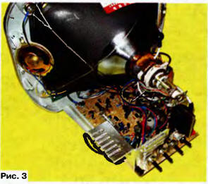
View of rear of the TV without the back cover is presented in Fig. 3.