


")

Continued
Videotrack MRCC collected on six chips: TDA8362, TDA8395, and TDA4661 three TDA6101Q. It includes a host of rejection, the demodulators of signals of different broadcasting systems, delay, matrix, switch inputs R, G, B, OSD device, the video amplifiers. The relationship of these devices shown in Fig.5. In videotrace the video signal is converted into chroma, and then to the color signals.
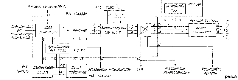
A feature of the chip is TDA8362 build bandstop and bandpass filters of channel chromaticity (filter "flared", etc.) without external coils, while in MC-2/3/31 TVs USCT for this we used six or seven customizable oscillatory circuit. If you do not take into account the video amplifiers, in videotrace there are no elements that can be configured.
Node of rejection cuts from the color video signal component C is the bandwidth occupied subcarrier chroma signals. Recall that in the NTSC subcarrier frequency is equal to 3.58 MHz, system PAL - 4.43 MHz. In the SECAM subcarrier - frequency and 4.25 4.406 MHz. Determination of the frequency, depending on the broadcast system occurs in the node automatically. The depth of rejection is 20 dB, which ensures effective cleaning the luminance signal from the chrominance subcarrier with a minimum width cut out the band. This increases the sharpness of the image. When receiving signal black-and-white image node of rejection and recognizes it off.
The luminance component Y is in the path synchronization in the matrix.
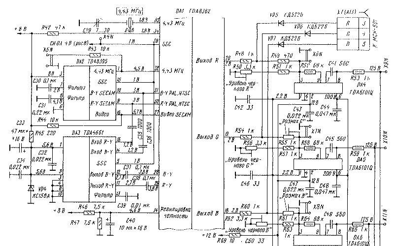
Color component is supplied to the demodulators. The demodulator signal systems PAL, NTSC is a chip of DA1. In the result of his work stand out color difference signals R-Y, B-Y, which via terminals 30 and 31 of the chip come in the delay line signals per string (chip DA3). In the NTSC signals are subjected to filtering processing, and PAL signals are averaged in two rows, one after the next another. From the output of the chip DA3 (pins 12 and 11) the processed signals R-Y, B-Y PAL & NTSC again returns to the chip DA1 via terminals 28 and 29.
Demodulator for SECAM signals contained in a chip of DA2. Via the output 27 of the chip the chip DA1 DA2 filed component C of the SECAM system, and o 32 circuits DA1 - signal frequency 4.43 MHz, necessary for the operation of the demodulator. The obtained chroma the signals R-Y, B-Y SECAM system from the terminals 9 and 10 chips DA3 also pass on the delay line, where the formation of the correct the sequence of direct and delayed lines in each of the chroma signals.
Coming from the chip DA3 signals R-Y, B-Y all systems on a chip DA1 after equalization time delay comes in matrix, where, mingling with the luminance component Y is converted into a color the signals R, G, B. After the findings 22-24 circuits DA1 to the switch come the signals R, G, B from an external source - computer (see Fig.3 and 4). A control switch is provided by input from the computer to the output 21 voltage blanking signal FB ("Window"). If it is missing, the output of the switch will pass signals with matrix, and FB<5 In - computer. Then, the signals R, G, B come on the weekend to the video amplifiers.
The video amplifiers (WU) are high voltage powerful operational amplifier TDA6101Q. Their main advantage - the broadband and the lack of powerful resistors in the output circuits (not more than 0.5 W). They have sensors system automatic white balance (ABB), but since the chip TDA8362 (unlike other versions) does not contain means for controlling the system of ABB, this function is not used.
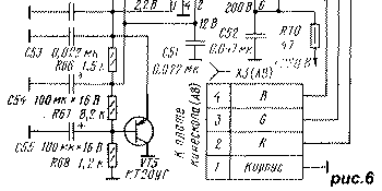
The work of WU and consider (Fig.6) for example the signal B. the output 18 of the chip DA1 input op amp (pin 3) DA6 the signal B is supplied through a divider R60-R63. Resistor R62 "Level black B" set the constant component of the output signal, equal to 125 V. the Resistor R61 "Span B" level variable component of the signal B with the same magnitude of the signal R. the Resistor R63 use when adjusting the white balance "in the black" (at the level blanking beams of the kinescope, and the resistor R61 - when adjusting the white balance "in the light" (normal brightness).
In the point of connection of resistors R60, R61 with the sit comes component of the B signal is displayed on the screen (OSD system). In a connection point of the resistors R61, R63 through resistor R64 passes the signal deep negative feedback from the output 9 of the chip DA6. Resistor R65 protects the amplifier from discharges occurring in the kinescope. Capacitor C49 adjusts the frequency response of the amplifier at high frequencies. Capacitors C51 and C52 - filtering in circuits supply voltage +12 and +220 V. the Capacitor C50 - filter in the circuit reference voltage +2.2 V required for stabilization mode amplifiers. It is formed by the stabilizer transistor VT5. Checkpoint X8N necessary when adjusting purity the colors and details of the beams of the kinescope. When the closure beam B is extinguished. Point X11N is used to check the level and shape of the signal applied to the kinescope.
The video amplifiers of the signals R and G are constructed analogously, except that in tract R the regulator of the magnitude of the signal no.
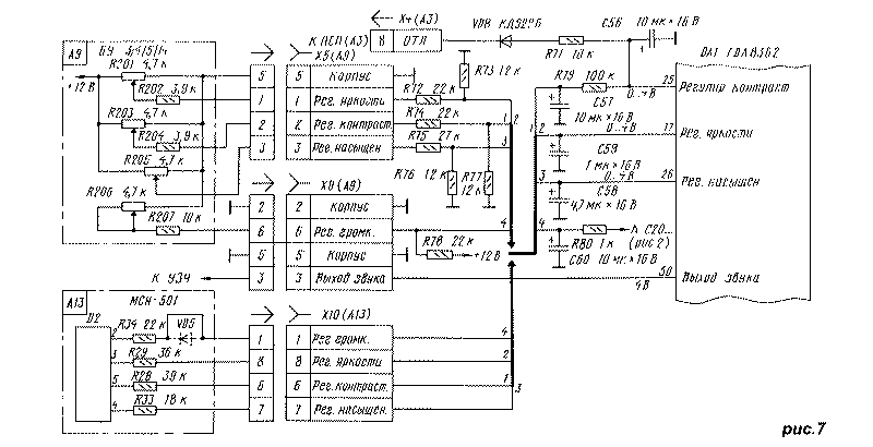
Connection chain adjustment parameters image and sound to MRCC shown in Fig.7.
Adjusting the volume in USCT provided the change of resistance of the resistors R206, R207 in the control unit (A9), connected between the micro-WPCS-1/2 in module MRK and common wire. When using chip TDA8362 adjustment occurs when the change voltage at its pin 5 within 0.1 3.9…V. To do this with a hovercraft or CCA included chain R80C60R78 together with resistors R207, R206 to BA. Resistor R207 (it's marked as R33 to BA-3/3-1, R7 to BA-4, R6 in BU-5 and R15 in BU-14) should have a resistance of 1 kOhm.
When using the sit regulating circuit the volume includes elements of R80, C60 and resistor R34 to the sit. In the sit diode VD5 completing the bridge, and the resistance of resistors R28, R29 should to be 18 ohms.
Brightness, contrast and saturation when the use of MRAs and USU continues to adjust variable resistors R201, R203, R205, located on the front panel of the TV. Since they engines removed for regulating the voltage in the range 0…12 V, and chip DA1 need to give a signal of not more than 5 In, after the contacts of the socket X5 (A9) included voltage dividers R72R73, R74R77, R75R76.
When using the sit all adjustments happen through the module with the remote control or keypad on the front the panel of the TV. All the adjusting resistors TV off.
In both cases (when using SVP, CCA or MSN) control voltage adjustments are transmitted to the terminals 17, 25, 26 chip on circuits, including filter capacitors C57-C59. When using MRAs, WUSU they stabilize the control voltage, and when working with ICSU average pulse signals adjustments variable duty cycle, generated by the module.
In the chain adjust the contrast using elements VD8, R71, C56 voltage current limiting rays (EX), reducing the amplitude of the signals R, G, B coming to WOO, increasing the total current rays above normal.
Any DIP resistors adjusting the colour tones are disabled.
Tract synchronization consists of the lower case and personnel singleselection, generator trigger pulses lowercase sweep (Sisep) and pulse staffing sweep.
In lower case sinhroselektora allocated lowercase sync from the luminance components Y of the video signal coming from switch video inputs. The signal Y, the stabilization of the amplitude of which was ensured effective radio channel AGC and a host of white spot inversion, is limited by the maximum and minimum so that the signal line and human extinction, as well as "flash" signal color synchronization is guaranteed to cut at any scale of brightness components Y.
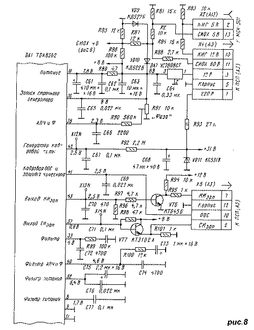
Peeled lowercase stable clock amplitude is received at the first loop of the PLL, correcting them the frequency of the pulses Sisap. The capture bandwidth synchronizing the first loop is equal to +/-900 Hz, and retention of captured synchronization +/-1200 Hz, which is significantly better than the corresponding indicators (+/-700 Hz) have chips KHA used in submodule FCP TVs USCT. The second loop of PLL horizontal, as usual, ensures the stability of the vertical position of the left border of the image. The resistor R91 "Phase" (Fig.8) allows you to properly set the phase image. The impulse Sisap amplitude 0.8 In with output 37 of the chip DA1 pass through the emitter follower to the transistor VT7 to pin 2 of connector X5 (A3) and later in the module lowercase sweep.
The pulses controlling the vertical sweep are formed in the chip DA1 from the sequence of pulses Sisap when dividing it by the number of rows in the half frame image (defined in the process of identification coding of the chrominance signals) with correction reference HR clock (XI) coming from HR sinhroselektora. Such a construction facilitates the search for the human clock in wide bandwidth (45…64.5 Hz) to their capture, which simultaneously leads to automatic adjustment of the pulse generator frame scanning when work on systems SECAM, PAL (50 Hz) and NTSC (60 Hz). As only 15 consistently came human clock (XI) will be to be within a wide swath, the system switches to narrow a streak that will continue. If six consecutive XI beyond the narrow strip, the device enters the search mode in their wide bandwidth.
Sawtooth pulses vertical blanking (CPN) the amplitude of 1.25…1.5 V are formed on the output 42 of the chip DA1 the integrating circuit R92C67, which are connected to the voltage +31, stabilized by Zener diode VD11. The linearity of the pulse is improved by the personnel supply voltage negative feedback (EP) amplitude 1 In arriving at the output 41 of the chip DA1 with sensor EP - resistor, in the circuit of personnel deflecting coils. In addition to improving the linearity of CIT sensor OOS performs the function of monitoring the output stage frame scanning. If the voltage across it is less than 1 In (open circuit personnel coils) or more than 4 In (faulty output stage), outputs R, G, B chip DA1 closed to avoid burn-through of the kinescope.
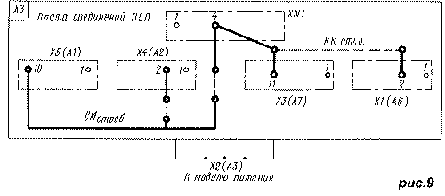
In TVs USCT signal personnel OOS formed in the module frame scanning MK-1-1 on the resistor R27. In the SRP Board (A3) is present on pin 2 of connector X1 (A6) and at pin 11 connector X3 (A7). To pass to MRCC, you can use released with the introduction of the module chain SISTROM, connecting pin 10 of connector X5 (A1) and the contacts 4 of the connector X4 (A2) and XN1 on the PSP. All of these chains is shown in Fig.9. For the proposal should be connected to the SRP pin 11 of connector X3 (A7) and pin 4 connector XN1 hinged jumper. In Fig.9 shows a Board with the printed conductors. The dashed line depicts the jumper, located on the side of the sockets.
In TVs with chip TDA8362 in the output cascade frame scanning is usually applied chip TDA3651/54 (CHA) or TDA3651Q/54Q (CHA) having a current control. HR the trigger pulse transmitted from the output 43 of the chip in such TDA8362 the output stage is a current pulse amplitude of at least 1 mA in the live of the beam and several microamperes during the return stroke. He corresponds to the voltage at pin 43 with level 5 In direct and 0.3 V At reverse, i.e., short runs the flyback pulses are directed down from the level of 5 V.
In TVs USCT management module MK-1-1 ensured a positive (upward) start the vertical scan amplitude of 10 V. For approval of the form and amplitude the pulses coming from the output 43 of the chip DA1, required for module MK-1-1 applied to the amplifier-inverter, collected on the transistor VT6 (Fig.8).
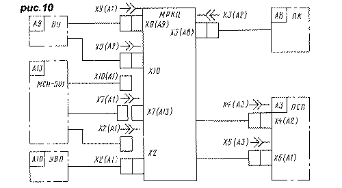
Connection diagram MRCC with other blocks TV USCT shown in Fig.10.
Before proceeding to the description of the module structure, consider possible modifications depending on the type of retrofit TV and wishes of its owner.
1. The channel selectors SC-M-24-2 and SC-D-24 will work successfully in MRCC, but their replacement with more modern all-wave selectors SC-B-618, KS-V-73 and especially UV-917 will allow significantly increase the sensitivity of the TV to improve the ratio signal/noise ratio and to simplify the module due to the direct (without transistor VT1) the connection of the selector with the filter ZQ1 (see Fig.2). The presence of these selectors combined antenna input for VHF and UHF eliminates the problem of connectivity two antenna inputs of the TV USCT distribution network collective admission.
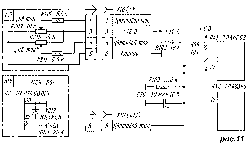
2. List of systems of color television, processed chip TDA8362, is determined by the voltage at its output 27. If it is greater than +5 V (pin 27 through a resistor R44 is connected to the conductor voltage of +8 V, as shown in Fig.6), the signals are processed only systems are SECAM and PAL. If there is a need in the treatment of any of NTSC, then the circuit connecting the output 27 of the chip should be mounted in a accordance with Fig.11, by setting the elements R102-R104, C78, VD12 and removing resistor R44.
When using UVP types of CCA, SVP controller the color tones NTSC (in this system operational needs such adjustment, since the change in the amplitude of the luminance signal causes the color change of the image) serves as a variable resistor R211 (Fig.11) - one of the two color tone knobs mounted on the housing TV.
When you sit facility for adjusting the color tone NTSC use untapped in standard switching on the synthesizer adjustment, output on pin 6 of the chip D2 of the sit. To do this, connect pin 6 of the chip D2 with 9 contact connector X10 sit through a resistor R104 the nominal value of 20 ohms. On the screen as symbols of adjustment will be to display a symbol of TONE (timbre). If desired, the designation can substitute the correct HUE (color), if you include the diode VD11 between pins 20 and 38 of the chip D2 of the sit, hotpaw the output 38 from the common wire.
All this will allow you to receive signals NTSC 4.43 with the video input.
As for signal system NTSC 3.58, taken with the antenna input, then they take serious the change of the radio. Should the inclusion of the passband and stopband filters at the frequency of 4.5 MHz. Parallel connection of three notch filters between the VT2 transistor and the output 13 of the chip DA1 (see Fig.2) will lead to the fact that the video will be cut too wide band frequencies that will degrade the sharpness of the image. To solve this problem in TV PANASONIC chassis MX3C [5] applied special chip that recognizes a standard composed of only one need a notch filter. Adding significantly more complex MRCC, therefore, it is not recommended.
3. The TV used the same USCT modules that USCT. The Pinout of all the connectors match up, and installation MRCC on these TVs does not cause additional problems.
4. This is not the case in the devices of the series USCT. Prior to making a module for them it is necessary to compare the Pinout connectors on the module Pinout reciprocal parts of the TV and make the necessary changes in MRCC. The following Board size module match the size of the cassette USCT and may not coincide with the dimensions of the chassis upgraded TV. might need a reflow of the Board MRCC. To give more specific recommendations are not possible, because unlike USCT schematic diagrams and PCB TVs USCT different factories not uniform and differ from each other. Offered guided factory circuit TV and upgraded reference [6].
5. In the TV OPENCT module MRCC quite can be used to replace the signal processing unit BOS provided plugins module UM1-3 (USC) and cascade quenching beams of the kinescope (both are barefoot). Another (relative to USCT) size cassette requires increasing the Board size without changing the pattern of printed conductors. When simultaneous replacement of the selector SC-In-1 (Ku which is lower than that of SC-M-24-2) on a more modern and DIP type SVP-4 Sit in OPENCT you can get all the TV's functions of the fifth generation.
6. In transition from OPENCT to USCT models USCT-P (it - OPENCT) module MRCC could replace the whole unit cost scan and signal processing TOLERANCE, which are the radio channels brightness and colour. It is installed the selector SC-M-24, modules UM1-1, UM1-2, UM1-3, UM1-4, UM2-1-1, UM2-2-1, UM2-3-1, UM2-4-1, M2-5-1. All of them, in addition to the selector and UM1-3, is not needed. Not needed and the synchronization module M3-1-1, mounted on the motherboard scan BROS. Replacement of this set of modules new (MRCC), of course, possible and desirable, but needs serious rework in the module, and the remaining Board BROS in connection with an entirely different system Board-to-Board connections and is not recommended.
Literature
4. Peskin, A., Konnov A. TVs foreign firms. The device adjustment, repair. A series of "Repair", vol.17 - M., Solomon, 1998.
5. Sokolov V., Pichugin Yu Repair colored stationary TVs USCT. A reference guide. MRD, vol. 1200. - M.: Radio and communication, 1994.
Publication: N. Bolshakov, rf.atnn.ru