


")

In order to reproduce a color image in the TV set it is necessary that the luminance and color difference signals come to the cathodes and control electrodes of the kinescope at the same time. It is known that the propagation time of a signal through a channel is inversely proportional to its bandwidth. The smaller the bandwidth of the channel, the more latency. Since the bandwidth of the chrominance channel is 6 MHz, and the color channel - 1.5 MHz, there is a delay of the chrominance signals by about 0.6 to 0.8 μs. Until recently as delay lines was used unregulated line type LSAS to 0.3/1000 (300 NS 1000 Ohms) or LSST-0,7-1500 (700 NS, 1500 Ω), which require careful coordination as input and output.
If the width of vertical color transitions, as a rule, does not exceed 2 mm even in the SECAM system (because of the coding features), because of a discrepancy between the midpoints of the front and rear fronts of the color-difference pulses with the means differences of the chrominance area of color transitions horizontally when receiving the signal from the air reaches 4…6 mm, and when working with video recorder can take up to 10 mm [1], which manifests itself as a "smearing" of the contours of brightly colored objects, the appearance of the frills of distorted color, "aproriate" small parts, etc.
To remedy this defect in the fifth generation TVs used color corrector definition Philips TDA4565, which block diagram is presented in Fig. 1. Using it in the TV fourth generation "Horizon TC", you can significantly improve the quality of the image. The corrector consists of two functional units:
- adjustable gyratory delay line for the luminance signal Y;
"obotrites" chroma pulse R-Y, B-Y.
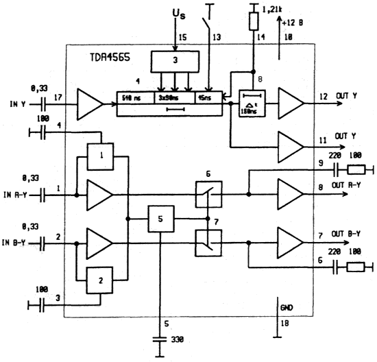
Fig. 1. Block diagram of the color corrector definition TDA4565
Giratina delay line 4 consists of 10 cells with a delay of 90 NS each, and one cell with a delay of 45 NS. 6 cell 90 of the national Assembly are combined into one unit with time delay 6x90=540 NS. They are followed by three cells, 90 NS, which are connected in series with the input unit of the electronic switch 3 (three of a threshold comparator with switching thresholds of 4.5±1 V, 7,5±1 V and 10.5±1), controlled by pin 15. Thus, increasing the voltage at pin 15 can incrementally increase the delay time of the signal to 270 MS. The additional delay 45 NS is enabled by the output circuit 13 to a common wire. Between pin 11 and pin 12 is the fixed delay 8 another 180 NS. Thus it is possible to adjust the delay for the luminance signal with a step 45 is not with output from 540 to 11 855 not(540 + 270 + 45 = 855), and output 12 - from 720 1035 NS to NS. Output stages (pins 11 and 12) made in the form of emitter followers with generators in the emitter circuit.
In obsterical color-difference pulses includes an edge detector pulses 1, 2; pulse shaper 5 and the switches 6, 7. The delay in the channel processing chroma signals is approximately 150 NS (100 to 200 NS). In moments of fronts and troughs chroma signals by differentiating and rectifying the outputs of the detectors are formed by pulses of positive polarity, the amplitude of which is proportional to the rate of change of the source signals. After the high pass filter and limiter 5 these pulses control the two identical channels-obotrites chroma signals, in the form of electronic switches 6 and 7. They commute paths R-Y and B-Y. the outputs of the keys connected storage capacitors. The "total" key management provides simultaneous change of colors in both channels at short color passages. The capacitors on pins 1 and 3 IC designed to suppress components outside the band of frequencies of color-difference signals, including residues subcarrier of the chrominance signals, which improves the signal/noise ratio. Output stages (findings 7 and 8) made in the form of emitter followers with kaskadnye generators of the current in the emitter circuit.
The values of the outer piping components are specified in accordance with the typical switching circuit. Learn more about work offset can be found in [2].
Circuit of the corrector (Fig. 2) is borrowed from TV's "Horizon". It is characterized by the presence of trimming resistors R5, R6 [3] the outputs of the signals B-Y and R-Y, by which tune the color balance. In modern TVs is a need for such regulators is eliminated, because the white balance is done automatically. From the model the scheme of inclusion of different values of RC-TSE-Pei, the time constant of which determines the length of the front, and have an active current source (AIT) on the transistor VT1. The input of the TIA through the differentiating capacitor 47 pF receives a chrominance signal ahead of 180 NS. AIT is in parallel with the internal generator of the current in the emitter circuit of the output stage. At such values of RC-circuits the duration of the color transitions (about 150 NS) roughly corresponds to the duration of brightness variations in the luminance channel (about 6 MHz).
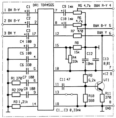
Fig. 2. The scheme of inclusion of a corrector
Resistor R3 should be chosen with an accuracy of ±1%, because the delay time is proportional to its resistance. In the case of chips TDA4565A resistance R3 to 1.15 ohms (in parallel with the resistor to 1.21 kOhm included 27 kω).
When the engine of the resistor R4 is in the highest position included one additional delay line 90 NS, in the middle position two 90 NS total delay of 180 NS), in the lowermost position three (270 NS).
Design and details. Drawing of the PCB for more submodule size 60x45 mm is depicted in Fig. 3, and the Assembly drawing in Fig. 4. Electrolytic capacitor C12 - type K53-4 to 20 V, and the rest - K50-35. Non-polar capacitors - type C-5. Trimmer resistors - SDR-38A.
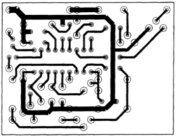
Fig. 3. The printed circuit Board
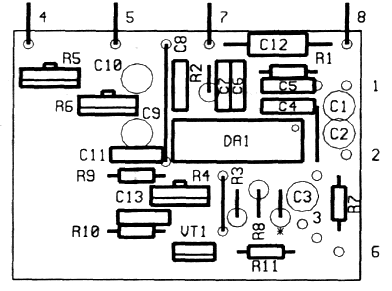
Fig. 4. Assembly drawing
Before mounting the submodule must be soldered to points 4, 5, 7 and 8 lead wires with a length of about 10 mm and unsolder from the main Board elements R38, R39, R42, R55, C31, C32, SPZ, VT2, VT3, and the delay line WT (LSAS to 0.3/1000) and elements of its approval R63 and R88. Resistor R60 150 Ω must be replaced by a resistor of 10 Ohms, capacitor C48 capacitance 22 UF - 0,047 UF. Near the connection point R60 and s and on the edge of the Board into a "common wire" on the same line with the upper pins (right diagram) of the capacitors C31 and SPZ drill the holes for connecting the power supply circuits (terminals 4 and 7) submodule.
Before mounting the submodule conclusion KN4 should be shortened by 2…3 mm, and the condenser C to bend down to the Board. Conclusions 4 and 5 of the sub module soldered directly to the main Board instead of the top findings of the removed capacitors C31 and the SPZ, and the points 1 and 2 connect the flexible wires (length 55 and 70 mm, respectively) with lower findings of these capacitors. Conclusion 3 submodule connected with shielded wire (150 mm) instead of the right of withdrawal of the removed resistor R88 and conclusion 6 - flexible wire (55 mm) o 2 removed delay lines.
Adjustment. When setting up a signal, "color bars" from the output of the corresponding generator at pin 1 XN2(A1), after removing the jumper. Give the signal at the RF-input (due to possible interference), and use the signal telecentre (due to the duplication of images) is not recommended. The delay line controlled via the resistor R4 and the bridge between the DA1 pin 13 and GND on the minimum area of color transitions in the horizontal direction. Color balance is set by the resistors R5 and R6. The optimal amplitude of the signal R-Y is about 1.05 V (the maximum is 1.5 V), the signal B-Y is about 1.33 In (1.9 In maximum).
Some TVs may submodule decoder SD-41 is replaced by a more modern, such as "electronics 016" or similar with regulators of signal levels at the outputs. In these blocks, these knobs should be set in the position corresponding to the maximum output signal, and optimal levels are set from the outputs of the corrector colour definition.
With careful setting of the corrector is observed a clear effect of increasing the clarity and purity of the image, it gets bumpy and purity. When there is insufficient brightness might need adjustment mode input stage gyratory delay line through resistor 220…510 ohms, connected between the terminals 17 and 16 DA1. This is determined by the best reproduction of the leftmost white band [3]. The specified resistor not shown in the diagram, but on the Board has a place for its installation.
Literature
Author: A. Petrov, D. Petrov, Mogilev; Publication: www.cxem.net