


")

Three decades ago, many radio Amateurs interested in ultra-long the reception of TV. How much work, skill and imagination were they, improving television receivers and creating a complex antenna system, allowed to "circumvent" the vagaries of radio wave propagation.
Satellite repeaters made it more "stable" channel of signal transmission, but technical implementation of the reception has not been simplified. Here hams there is a place to apply their knowledge and skill. The article describes Amateur Converter, the parameters of which are not inferior to the best examples industrial production.
The author developed a Converter is designed to operate in systems receiving satellite TV Ku band (10,95 …to 12.0 GHz) with a single frequency conversion.
Converter has the following specifications:
- Operating frequency range, GHz - 10,95 12,0…
- Intermediate frequency, MHz 950 2000…
- The typical noise figure, dB - 0,6
- The transmission coefficient, dB - 60
- The frequency of the local oscillator GHz - 10,0
- The voltage, V - 13/18V
- Current consumption, mA, not more than 95
- The polarization of the input signal - vertical/horizontal.
The Converter is built on a low-noise frequency Converter, structural combined with the feedhorn of the antenna system and built-in switch the polarization of the input signal. Its schematic diagram is shown in Fig. 1. It consists of an input waveguide with sunken probes (electric not shown), the microwave amplifier, transistors VT1 - VТЗ, bandpass filter using strip lines L9 - L18, lo frequency of 10.0 GHz transistor VT4 with frequency stabilization, balanced mixer on VD2 diode Assembly, amplifier intermediate frequency on chips DA2 and DA3, the voltage regulator on the chip DA4. It includes also the device on the chip DA1 performing the functions of a voltage Converter +5 In at -2 V, the polarization switch and stabilizing currents of the FETs VT1 - VT3. In the Converter applied microcircuits, transistors and diode assemblies manufactured by Hewlett Packard (USA).
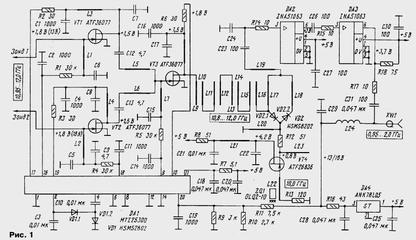
The input signal is focused by a parabolic mirror, enters the radiator and from it - in a circular waveguide with a diameter of 19 mm. the Connection of the strip lines paddles transistors VT1 and VT2 to the waveguide by using an immersed probe, by 90 degrees in a waveguide that allows you to receive signals both vertical and horizontal polarization. Switch the polarization Converter is the supply voltage of 13/18 V DC coming by cable to the output connector XW1. The voltage across the divider the resistors R9 - R11 is input to the comparator circuits DA1. When the voltage power 13 In DA1 chip includes the VT1 transistor and its drain appears a voltage of +1.5 V. the Transistor VT2 is at this time closed negative a voltage of -2 V, arriving at its gate, and, furthermore, the voltage from the drain this transistor is removed.
When switching the supply voltage of +18 In the transistor VT1 is closed, and the VT2 transistor is switched on in normal operation. This allows electronic way to change the appearance of the polarization of the received signal.
The summation of the signals from the transistors VT1 and VT2 by using the bridge strip lines L5, L6. The total signal is supplied to the gate of the transistor VT3 - the second amplification stage. Transistors VT1 - VT3 type ATF36077 have a gain of 12 dB at a frequency of 12 GHz at a voltage of +1.5 V and current is 10 mA. Thus, the total gain of the microwave amplifier is 24 dB with noise figure of 0.5 dB.
For best value noise ratio fine tuning is needed the mode of operation of transistors and coordination of their inputs and outputs. In reality it is possible to obtain the noise factor is different from passport 0.1 dB, so in characteristics provides the maximum value of Cs at a frequency of 12 GHz 0.6 dB.
The amplified microwave signal from the drain of the transistor VT3 is input to bandpass filter L9 - L18 performed on stripline interdigital resonators and having a bandwidth of 10.8… to 12.0 GHz with uneven frequency response H dB.
Output of the filter the microwave signal is fed to the input of balanced mixer made on VD2 diode Assembly for microwave diodes with Schottky barrier strip and the bridge. On the other the balanced input of the mixer receives a signal with a frequency of 10 GHz from the output of the local oscillator transistor VT4.
The local oscillator is made on a field-effect transistor with a common drain and open a half-wave resonator in the circuit, the gate-source of the transistor, and stabilizing high-q cylindrical cavity of ZQ1 titanate-barium ceramics.
Loss of signal conversion is about 7 dB. The intermediate signal frequency Fпч from the output of the balanced mixer through the filter elements L19, C23, C24, R14 is supplied to the input circuit DA2 preliminary if amplifier, executed according to the scheme given in the journal Instruments and experimental techniques", 1984, № 2, p. 111 (Abramov, F. G., Volkov, Y., Vonsovskii N. N. "Agreed broadband amplifier"). The amplifier on the chip has a range INA51063 operating frequencies of 100..2400 MHz at a gain of 22 dB. Output preliminary if amplifier the signal is fed to the input terminal of the if amplifier, made on the chip DA3 and having an operating frequency range of 100…3000 MHz at a gain of 23 dB. Resistors R14, R15, R17 resistance of 10 Ohms prevent self-excitation cascade amplifiers included, especially when the misalignment of the load connected to the connector XW1.
The Converter power supply is provided from the integrated stabilizer DA4, to ensure stabilization of the voltage of +5 V at currents up to 150 mA.
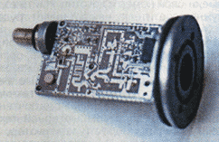
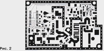
Converter (apart from the input waveguide) formed on the printed circuit Board (Fig. 2) from double sided foil fluoropolymer FAT thickness of 1 mm.
Location conductors and components on the Board shown in Fig. 3.
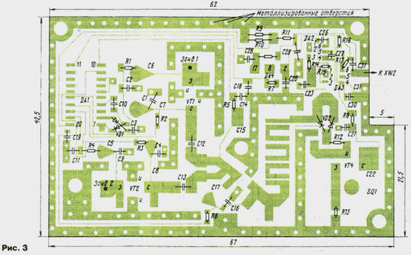
Hanging items are from the printed conductors, foil return side of the card is used as a common power bus. It is important that all details had minimum possible length of the pins; they should be installed directly soldering on the wires. For the connection of conductors of a shared bus power, which are arranged with side parts, with foil back side the Board, in it drill a series of metallized holes.
The Converter is used, the resistors R1-12 with power dissipation of 0.125 watts. Perhaps the use of resistors of this type with a capacity 0,062 W and resistors R1-8 with a capacity of 0.125 and 0.25 watts.
In low frequency circuits and power circuits used type capacitors K10-47C. Capacitors C9, C12 and C13 - K10-42. Capacitors in high frequency circuits, capacity of which is not specified (C5 - C8, C15, C17, C22, C24), made "print" method - their capacity plates is formed of a special form printed track and the shared bus power supply Board material as the dielectric. High-frequency connector XW1 type F-75 (available at radio countries CIS).
Transistors, diode assemblies and circuits - Hewlett-Packard company (USA). In as VT4 is possible to use transistors APA-2 and APA-2, transistors VT1-VT3 interchangeable similar production of Siemens, NEC, Philips or APA-2 and PA-2, however, in the latter case, some increase coefficient the noise of the Converter. Diode Assembly HSMS2802 (VD1) can be replaced with two diodes KDA or CDA and the Assembly HSMS8202 (VD2) - two diodes CAA or CAAR. Instead of the integrated stabilizer 78L05 suitable CREA, KREN, KREN. When replacing the resonator ZQ1 should use TSBN-10.
To connect submersible probes (probe 1 and probe 2) to the gates of transistors VT1, VT2 boards in drilled holes with a diameter of 2 mm, and the foil on the lower side Board removed around the holes in a radius of 2 mm from the centre of the installation. Probes fixed in the housing bore (Fig. 4, view a-A) a fluoroplastic bushings with a diameter of 4 and a length of 3.5 mm. the Resonator ZQ1 glued to the PCB with a thin layer of glue, made from Plexiglas dissolved in dichloroethane.
Installation of elements on the Board perform low-voltage soldering iron with grounded tip solder marks RSTP 50-18 or POI.
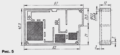
Fully charge made with mounted elements are placed in cast or milled body (see Fig. 4), the author used from ready similar products Microelectronics Inc. The body is made of alloy aluminum (silumin, duralumin, etc.) and closed the top cover (Fig. 5), bolted to the housing by screws M2. Cover milled or cast provides the division of the Board into compartments and prevents the formation of parasitic reverse connections and leakage of the lo signal to the input of the microwave amplifier.
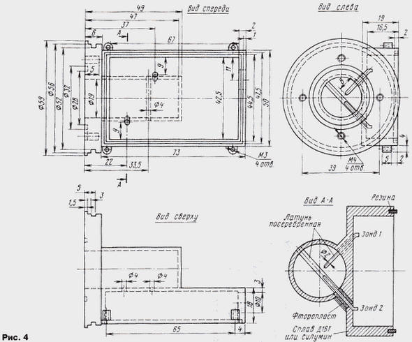
In the manufacture of the Converter in Amateur conditions, you can use a simplified version of the case. To do this on a lathe is necessary for Fig. 4 to grind the flange to the waveguide made of brass and soldered box mounting Board, bent from sheet brass. The lid is also made from sheet brass and in the right places napaimiut her partition to divide the trunking into compartments.
To prevent the excitation of parasitic oscillations in the compartments of the Converter to the inside of the lid in indicated in Fig. 5 locations (hatched areas) glued pieces of rubber 3 mm thick and coated with an absorbing layer of a mixture of carbonyl iron powder mixed with glue BF. In the cover opposite the end surface of the resonator drilled hole (not shown in the drawing, it the precise place after the installation of the resonator) and threaded M5 for brass the adjusting screw. It provides fine-tuning of the lo frequency by changing the distance between the screw (corps) and the resonator ZQ1. Deleting screw from the resonator frequency of the oscillator decreases, while zooming in increases. Therefore, before configuring the Converter needs adjusting screw to be wound only on the first few threads of the thread.
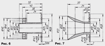
For sealing of the Converter is provided by the second cover and rubber gasket, laid in a groove in the housing of the Converter (see Fig. 4). Waveguide the flange of the Converter is connected to the flange of the radiator installed in the focus antenna with four M4 screws. Sealing of the waveguide is accomplished by install the rubber gasket in the groove of the flange of the Converter and PTFE film thickness 10…20 µm between the flanges. Drawings of feeds for Prime focus and offset antennas is shown in Fig. 6 and Fig. 7, respectively.
The configuration of the Converter is carried out in the following sequence. Connector XW1 connect regulated power supply +10…20 V DC with output current not less than 100 mA. Sets the supply voltage +13 V and is measured by a voltmeter the voltage at the terminals of the transistors and circuits. Their values must be different from of these not more than 10 %, otherwise replace the defective element. Further, increasing the supply voltage up to +18 B, we see that the comparator and switched on the drain of the transistor VT2 appeared a voltage of +1.5 V, and the drain of the transistor VT1, the voltage has become equal to zero.
To instantly check availability of the microwave voltage at the output of the local oscillator (lo), upper ( scheme) conclusion of the resistor R12 is connected millivoltmeter microwave (and millivoltmeter, described in the magazine "Radio", 1995, № 9, p. 40) and is satisfied the presence of microwave oscillations. To accurately measure the amplitude of the incident wave from the local oscillator is not possible, but if the readings of the millivoltmeter lie within 10…70 mV, the local oscillator is working.
Connect a DC millivoltmeter to the left on the diagram the capacitor tube C23, to check availability at this point the device is a small DC voltage (2…10 mV). This demonstrates a health balanced mixer (perfect to pick up a couple of diodes and balance the bridge is almost impossible).
After that, the Converter is closed by the first cover and connected to the antenna feed antenna on the one side and to the tuner on the other. Restructuring tuner find one received channels. The adjusting screw sets the exact frequency value lo 10 GHz %1 MHz, obtained by comparing the frequency with a known frequency a given channel. The Converter then close the second lid and seal.
Author: V. Zhuk, Minsk